Overview AI Launches Unified Inspection for High-Density Connectors
As next-generation compute systems pack more power into tighter spaces, the connectors that link their subsystems are becoming smaller, denser, and far harder to inspect. Overview AI today introduces a unified AI inspection capability purpose-built for high-density blind-mate connectors, delivering production-grade accuracy from the very first shift, across every manufacturing site.
The Growing Challenge of Dense Connector Arrays
Modern compute architectures, from hyperscale AI servers to edge-deployed inference cards, increasingly depend on high-density connector arrays to simplify assembly and modularize high-performance subsystems. Whether mounted at the midplane or backplane, a single connector module can carry hundreds or even thousands of individual pins. A microscopic bend on just one of those pins can cascade into complete system failure, or worse, destroy an expensive mating PCBA on the opposite side.
The challenge is compounded by limited physical access. Blind-mate designs are engineered so that operators never see the pin array once it enters the housing. That means defects introduced during handling, insertion, or shipping are virtually invisible to the human eye at production speed, making manual inspection inconsistent and unreliable at scale.
Why Traditional AOI Falls Short on Dense Connectors
Conventional Automated Optical Inspection (AOI) relies on hand-crafted rules: threshold-based brightness checks, edge-detection filters, and template matching. These techniques were designed for relatively simple, well-lit, and repeatable scenarios. High-density connectors break every one of those assumptions.
Extreme Pin Density
Hundreds of contacts packed into a few square centimeters create overlapping shadows and reflection patterns that confuse rule-based algorithms.
Subtle Defect Signatures
Pin deformations of 50–100 µm are invisible to threshold filters but catastrophic in operation. Deep learning excels at recognizing these sub-pixel anomalies.
Varied Defect Modes
Debris, surface damage, bent pins, and retracted contacts all look different. A single rule set cannot cover them without generating excessive false positives.
Limited Physical Access
Blind-mate connectors restrict the angle and distance at which cameras can capture images, reducing the effectiveness of conventional multi-angle AOI setups.
How Overview AI's Unified Inspection Works
Overview AI's approach replaces the one-model-per-location paradigm with a single, pooled deep-learning model that treats every pin position as a contribution to a shared feature space. The result is an inspection system that learns faster, generalizes better, and ships production-ready on day one.
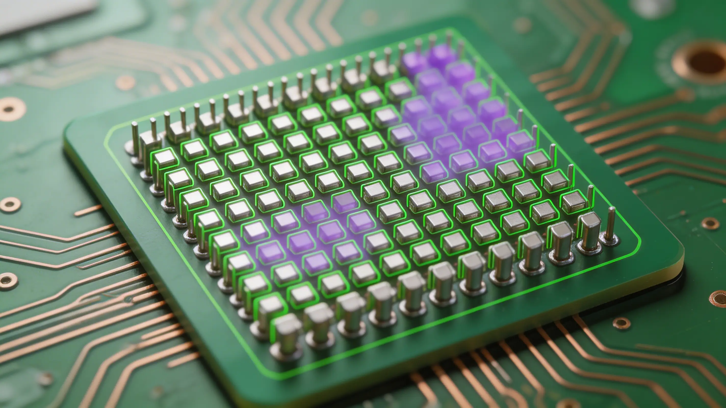
Architecture Diagram
Unified Model: Pooled Deep-Learning Across All Pin Positions
A single AI model shares learned features across all connector pin positions — enabling faster training, better generalization, and day-one production readiness.
Pooled Learning Across Every Pin
Instead of training a separate classifier for each pin location, Overview AI aggregates labeled examples from all positions into one shared model. This means every damaged pin the system encounters, regardless of location, strengthens the entire model at once.
Full-Array Inspection in a Single Pass
The system captures and analyzes an entire connector array, hundreds of pins, in a single high-resolution image pass, delivering in-line pass/fail judgments in under 30 seconds with no manual intervention.
Continuous Model Improvement
Every inspection result feeds back into Overview AI's engineering and quality platform, creating a continuously improving loop. As more data flows through the system, the model automatically refines its accuracy without requiring engineers to manually retrain.
Global Deployment from a Single Model
Engineers can take a validated model and deploy it across different SKUs, product families, and manufacturing facilities worldwide. One model, one standard, no per-site recalibration required.
Comprehensive Multi-Defect Coverage
Unlike systems that require separate models for each defect type, Overview AI's unified approach flexibly adapts to the full spectrum of connector defects within a single inspection pass:
Pin Deformation
Bent, twisted, or tilted pins caught before mating
Foreign Debris
Particles, dust, and contamination in pin cavities
Surface Damage
Scratches, dents, and plating wear on contact surfaces
Missing or Retracted Pins
Absent or push-back pins identified automatically
Production-Validated Results
Initial production deployments on next-generation AI compute platforms, including PCBA-level (L6) and tray-level (L10) assemblies, have demonstrated the system's readiness for high-volume manufacturing:
99.9%
Detection Accuracy
Validated in live production
<30s
Per-Connector Cycle Time
Full-array analysis inline
Day 1
Production Ready
No per-site recalibration
What This Means for OEMs and Contract Manufacturers
By replacing inconsistent manual inspection with Overview AI's automated, unified approach, compute system manufacturers can:
Boost First-Pass Yield
Catch damaged connectors before integration and test, eliminating rework cycles that slow production.
Reduce Scrap and Rework Costs
Identify and correct the upstream process steps that introduce pin damage, driving down defect rates over time.
Enforce a Global Quality Standard
Deploy one inspection model across every line, site, and contract manufacturing partner, ensuring consistency worldwide.
Govern Supplier Performance with Data
Use Overview AI's quality platform to set thresholds, track trends, and validate supplier adherence to your connector quality specifications.
Frequently Asked Questions
Q: How does Overview AI inspect hundreds of pins in a single pass?
A: Our unified model treats each pin location as part of a shared feature space. Instead of training a separate model per pin, every pin contributes to a single deep-learning model that learns common defect signatures, debris, deformation, and damage, allowing full-array inspection in under 30 seconds.
Q: Can the same model be used across different factories?
A: Yes. Because the model is trained on pooled data from all pin positions and defect types, it generalizes across SKUs, product lines, and factory locations. Engineers deploy a single validated model globally with no per-site recalibration.
Q: What types of defects does it catch?
A: The system detects pin deformation, foreign debris, surface damage, misalignment, and missing or retracted pins, and all within a single unified model, with flexible tuning to prioritize the defect modes that matter most for your product.
Q: Does this replace traditional AOI?
A: For high-density blind-mate connectors, Overview AI's approach significantly outperforms rule-based AOI. It can serve as a full replacement or as a dedicated secondary inspection layer for the connector types that legacy systems consistently miss. Learn more about connector inspection for zero-defect PCBA manufacturing.
Related Reading
Explore more about AI-powered connector and pin inspection:
Ready to Inspect Every Pin, Every Time?
Stop letting microscopic pin defects become million-dollar field failures. See how Overview AI's unified inspection model delivers 99.9% accuracy from day one, across every line and every site.
Schedule a Demo