
First-Pass Yield on the Line: AI Vision for Electronics & PCB Assembly
October 7, 2025 · 8 min read
Quick Answer
Electronics manufacturers lose yield to hidden defects like solder bridges, tombstones, and polarity errors. These failures often slip through traditional AOI systems because rule-based vision can't handle component variation, board warp, or lighting shifts. AI vision trained on real-world variation inspects consistently, explains decisions, and keeps up with takt time - directly at the edge.
Why Legacy AOI Rules Break
Rule-based Automated Optical Inspection (AOI) systems rely on geometry templates, pixel thresholds, and library matching. They perform well on ideal samples - and fail the moment reality changes.
Common pain points engineers know all too well:
Board warp and lighting drift
Even slight flex or glare alters reflected edges and leads to false rejects or missed solder bridges.
Component tolerance
Every lot brings micro-shifts in pad alignment, stencil spread, and component height that break rigid rules.
Novel defect types
Rule libraries can't anticipate new solder behaviors such as "head-in-pillow" or micro-bridges from paste inconsistencies.
Throughput sensitivity
Classic AOI slows dramatically when image complexity increases or when extra checks are bolted on.
The result: inconsistent first-pass yield, manual review queues overflowing, and engineers spending hours tuning thresholds instead of improving process capability.
What Changes with AI Vision
Modern AI vision systems learn from variation instead of fighting it. Overview.ai's architecture takes the same data AOI already collects and turns it into a continuously improving inspection model.
1. Pattern Awareness for Solder Anomalies
Deep vision models recognize spatial and texture patterns, not just edges. That means they can distinguish between a legitimate fillet and a bridge caused by excess paste or reflow shadowing - even under mixed lighting.
2. Pose Tolerance
By learning across rotations, flex, and lighting conditions, AI vision keeps detection stable when boards warp slightly or when fixture tolerances loosen over time. Engineers no longer rewrite rules for every new board lot.
3. Edge Inference for Real-Time Reliability
All inference runs locally on the Edge Node, so results return in sub-second time, protecting takt. Images never leave the facility; models sync only when approved, through Central Control governance.
Implementation Guide: From Pilot to Production
Component Class Capture
Gather representative images per component class (ICs, passives, connectors) under multiple lighting angles.
Defect Labeling
Mark solder bridges, opens, tombstones, polarity errors; confirm labels via dual-review for QA consistency.
Per-Class Metrics
Track precision/recall separately for bridges, opens, polarity; optimize thresholds based on cost of escape.
Weekly Threshold Review
Plot FP/FN trendlines to detect drift; retrain only on verified edge cases.
Versioned Rollouts
Deploy models gradually through Policy/Version control, validating on one Vision Station before fleet-wide push.
Each step reinforces reliability while minimizing disruption. Typical ramp-up to production readiness is under two weeks for a single line.
Outcomes: Measured, Auditable, Sustainable
Higher First-Pass Yield
AI reduces false negatives by learning from early process variation - fewer escapes, less manual review.
Fewer False Rejects
Tolerant thresholds prevent over-sorting when lighting or paste conditions drift.
Faster Root Cause Analysis
Overlays highlight which joint or component triggered the fail; operators resolve and retrain faster.
Stable Throughput
Edge inference maintains takt time without reliance on cloud latency.
Frequently Asked Questions
Why do rule-based AOI systems miss solder defects that AI vision catches?
Rule-based AOI relies on geometry templates, pixel thresholds, and library matching that perform well on ideal samples but break with board warp, lighting drift, and component tolerance shifts. AI vision learns spatial and texture patterns, so it can distinguish a legitimate fillet from a bridge caused by excess paste or reflow shadowing even under mixed lighting.
Does AI vision inspection slow down takt time?
No. All inference runs locally on the Edge Node, so results return in sub-second time and protect takt. Images never leave the facility, and models sync only when approved through Central Control governance.
How long does it take to get an AI vision model into production on a PCB line?
Typical ramp-up to production readiness is under two weeks for a single line. The path runs from component class capture and defect labeling through per-class metrics, weekly threshold review, and versioned rollouts validated on one Vision Station before a fleet-wide push.
What outcomes can manufacturers expect from AI vision PCB inspection?
Manufacturers see higher first-pass yield from fewer false negatives, fewer false rejects when lighting or paste conditions drift, faster root cause analysis through overlays that highlight the failing joint, and stable throughput because edge inference avoids cloud latency.
Related Reading
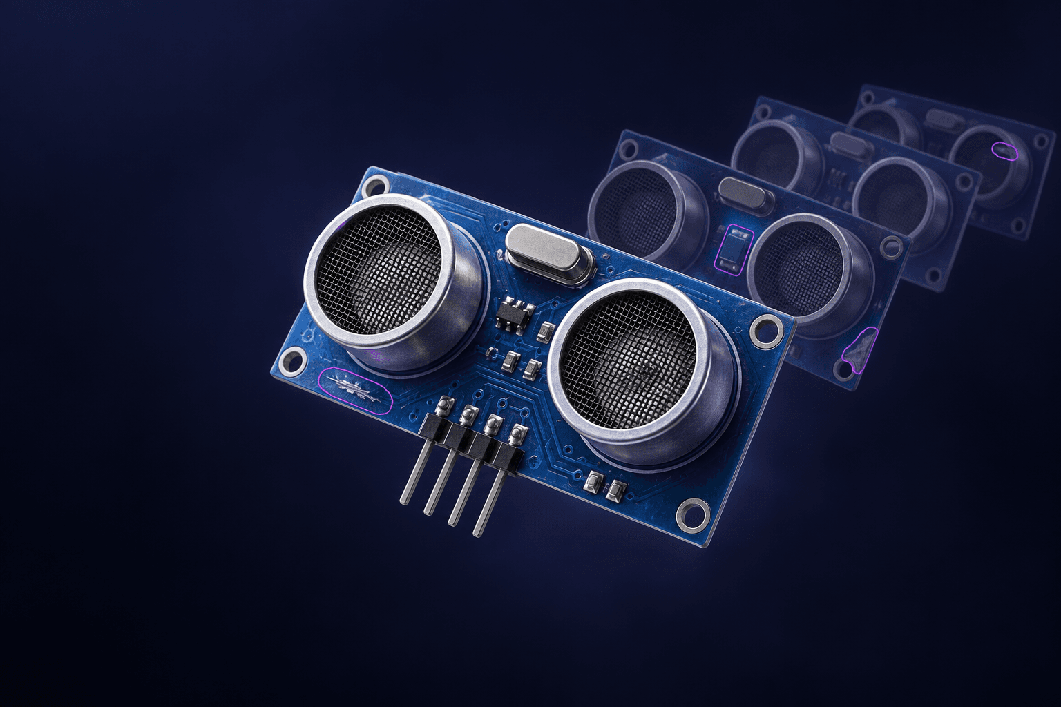
Can You Train a Defect Detection Model with Synthetic Data?
Our VisA PCB1 benchmark: 10 real defect images plus 50 generated matched an 84% real-data benchmark on one seed and reached 86% on another.
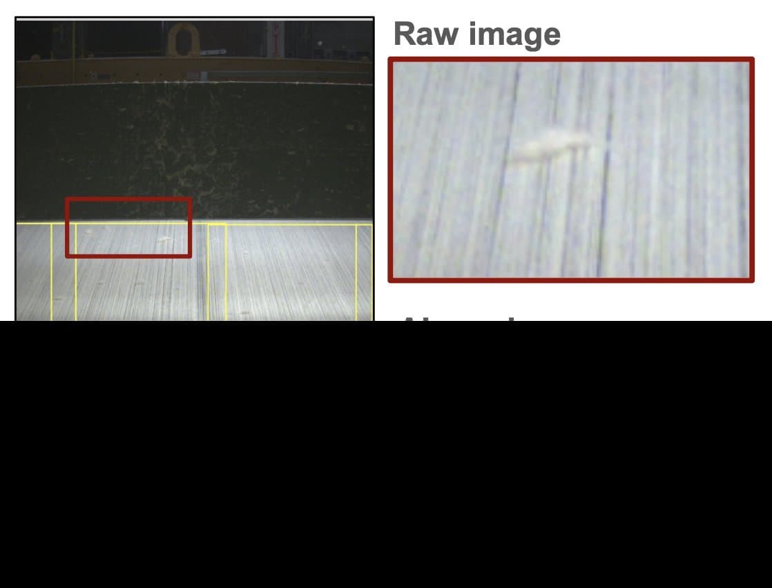
Anomaly Detection: Inspecting With Only Good Samples
How unsupervised anomaly detection finds defects you have never photographed, why it suits textured and low volume parts, and the cases where a trained defect model is still the better answer.
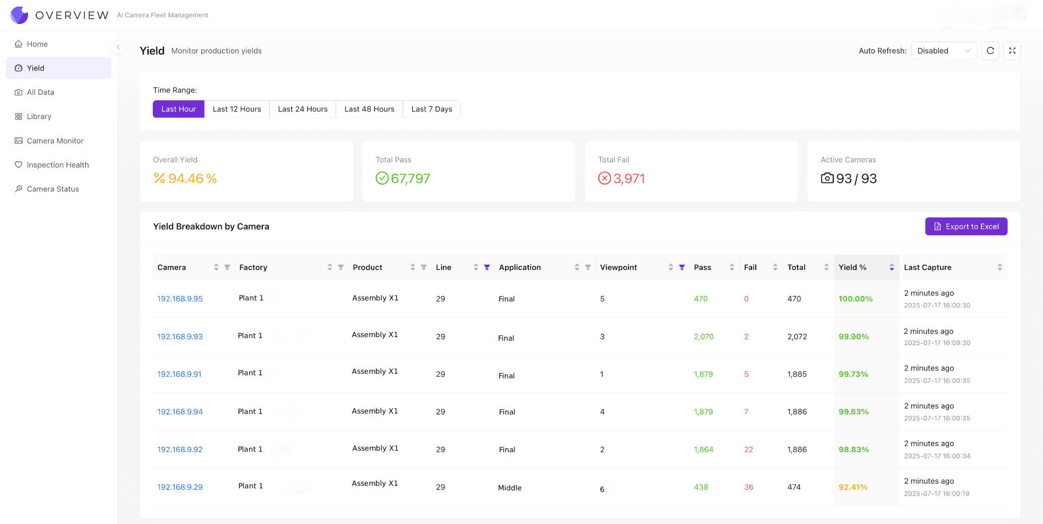
Backtesting an Inspection: Proving It Works Before It Ships
How to validate a vision recipe offline against known parts, build a test set that does not flatter you, and run a repeatability study on an AI inspection before it gates production.
Ready to Transform Your PCB Inspection?
See how AI vision can improve your first-pass yield and reduce false rejects on your production line.
Schedule a DemoSee how Overview AI inspects PCB solder defects
Send us a photo of your part or defect and a vision engineer will tell you whether Overview can catch it, with most systems deployed on the line in days.
Related Articles
AOI vs AI Vision in PCB and Electronics Manufacturing
Where rule-based AOI still wins, where deep learning beats it, and the false reject economics that decide the choice.
Read More →Connector Inspection: Achieving Zero-Defect PCBA Manufacturing
How AI vision detects bent pins, terminal seating issues, and solder anomalies for zero-defect PCBA lines.
Read More →AI Vision for Semiconductor Wafer Inspection
Detecting sub-micron wafer and die defects to protect yield across advanced chip production.
Read More →