
PCB & FPCInspection
Catch what AOI misses. Missing components, polarity flips, trace damage on flex, contamination, and cosmetic flaws on populated boards. One platform, every defect class, every product variant.
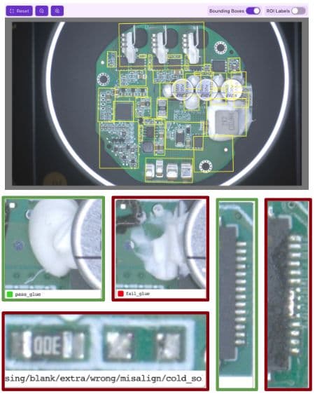
Glue, solder, components, and connectors on one PCBA
Where Our Cameras Inspect Boards
Real defect imagery from automotive, connector, and consumer electronics lines.
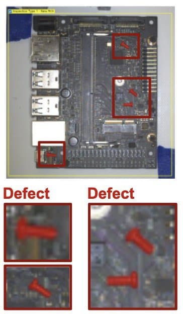
Foreign objects flagged on a populated board
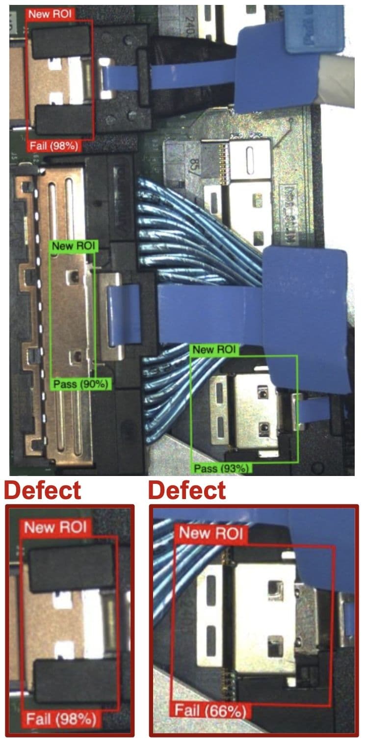
Per-connector Pass/Fail on cable assemblies
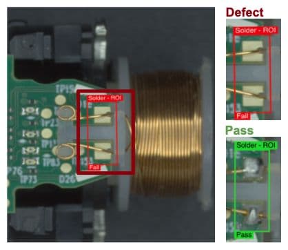
Real AI Solder-ROI Pass and Defect calls
PCB & FPC Defects We Catch
Populated PCBA Inspection
Inspect placed components for presence, orientation, polarity, and skew on every assembly that comes off the SMT line. The model trains on a few dozen reference boards and reliably flags missing capacitors, flipped ICs, tombstoned passives, and misaligned connectors. Recipe creation that took weeks on conventional AOI takes a single shift.
FPC and Rigid-Flex Defect Detection
Flex circuits expose unique failure modes: trace damage at the bend radius, coverlay delamination, scratches on the polyimide, and contamination in the gold pad areas. Overview AI handles the reflective and curved surfaces that defeat structured-light AOI, and the same workflow extends to rigid-flex hybrids without separate recipes.
Solder Joint & Conformal Coating QC
Cold joints, solder bridges, voiding, and conformal coating misses fail downstream test or, worse, escape to the field. The same AI model that inspects component placement also scores joint quality and coating coverage, with pass/fail at the joint level and trend data exported to your MES.
Cosmetic Defects, Scratches, and Markings
Visible scratches, solder mask scuffs, silkscreen errors, lot code legibility, and barcode quality all matter for high-end consumer electronics and medical devices. Our vision system unifies cosmetic inspection and OCR validation on a single platform, eliminating the parallel inspection stations that traditionally split these checks across separate vendors.
Unified PCB & FPC Inspection
One platform, every defect class, every board variant.
Hot Swap Between Variants
Switch board variants without recipe re-engineering. The model handles geometric variation gracefully.
SPC and MES Export
Every joint, every defect, every cycle logged to your existing systems. Native EtherNet/IP, Profinet, Modbus TCP, and REST.
Haystack Discovery
Surface anomalies you did not know to look for. Then retrain to catch them in production, without a vendor.
FAQ
Frequently asked questions
How is this different from traditional AOI?
Traditional automated optical inspection is rule-based and very good at what it was programmed for: component presence, placement offset, polarity marks, and solder volume against a threshold. It struggles when the defect is a judgment about appearance rather than a measurement, and it needs reprogramming for every new board. An AI approach learns from example boards instead, which shortens changeover on short product cycles and handles the cosmetic and mixed defects rules describe badly. Most real lines end up using both, rules where the tolerance is numeric and a model where it is visual.
Why are flex circuits harder than rigid boards?
Because they do not sit flat. On a rigid board the working distance is constant, so you set focus once and resolution is the binding constraint. A flex circuit curls and lifts, so the distance from the lens changes across the part and depth of field becomes the limit instead. You either constrain the part mechanically, close the aperture and add light to buy depth of field, or accept multiple captures. It is a lighting and optics problem before it is a software problem.
Can one camera cover a whole dense board?
Often not, and it is better to find that out with arithmetic than after buying. A board is physically large while its features are very small, so a single field of view wide enough to see the board leaves too few pixels on the smallest feature. Either use several cameras or several positions, or inspect at the region level where the small features actually are. The mixed reflectivity of a board is a second reason to split it up: an exposure that suits matte laminate tends to blow out bright solder in the same frame.
Ready to Replace Your AOI Black Box?
See the same boards, same defects, modeled by our team and your team in the same week.