Connectors & Electronics
Eliminate the Microscopic Flaws That Cause Field Failures

In connector and electronics manufacturing, you're in a constant battle against microscopic defects that can cause catastrophic field failures. A single bent pin, contaminated terminal, or misaligned contact can render critical automotive and industrial systems inoperable. You need precision inspection that catches submillimeter defects, but you can't afford months of integration time for a new inspection system.
Overview.ai is built for speed—both in production and deployment. Empower your operators to set up and run advanced connector inspections, catching pin defects, housing cracks, debris, and assembly errors that traditional AOI systems miss, with no coding required.
Defect Detection Capabilities
- Laser Welding Defects: Detect weld porosity, incomplete fusion, spatter, and heat-affected zone anomalies in precision laser welding operations
- Soldering Defects: Identify solder bridging, cold joints, insufficient solder, tombstoning, and head-in-pillow defects on PCBAs
- Debris & Foreign Objects: Detect foreign object debris (FOD), dust particles, and contamination that can cause short circuits or reliability issues
- Metal Contaminants: Find metallic particles, solder balls, and conductive debris that pose critical reliability risks in electronic assemblies
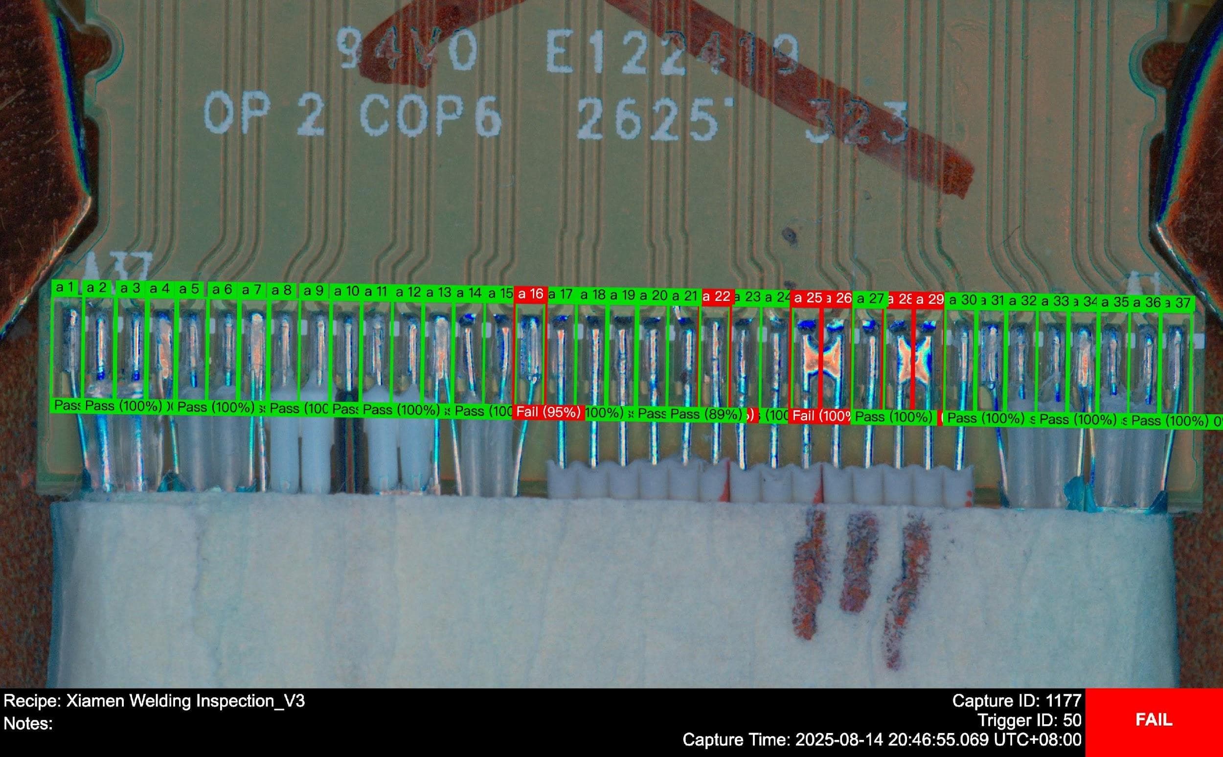
- Pin Checking & Inspection: Verify pin presence, alignment, bent pins, missing pins, and coplanarity in connectors and semiconductor packages
Why Overview.ai for Connectors?
Overview.ai is built for speed and accuracy. Increase first pass yield (FPY), reduce costly rework, and protect your brand from the fallout of device failures. Solve complex inspection challenges in hours, not weeks, and get actionable data to fine-tune your SMT line and upstream processes.
- Powerful edge AI models powered by on-board NVIDIA GPU
- AI explainability tools like Haystack to improve & refine models
- Storage for 20k+ in-production images to detect new defects
- No coding required—train on your specific defects
- Real-time edge processing & MES/PLC integration
Key Applications
SMT & PCB Inspection
Go beyond standard AOI. Our AI can identify defects that rule-based systems miss, such as subtle solder bridging, insufficient paste, tombstoning, and "black pad" defects on BGAs, dramatically reducing false positives.
Laser Welding Quality Control
Ensure weld integrity in battery modules, sensor assemblies, and microelectronics. Detect porosity, spatter, incomplete penetration, and heat-affected zone defects in real-time to prevent field failures.
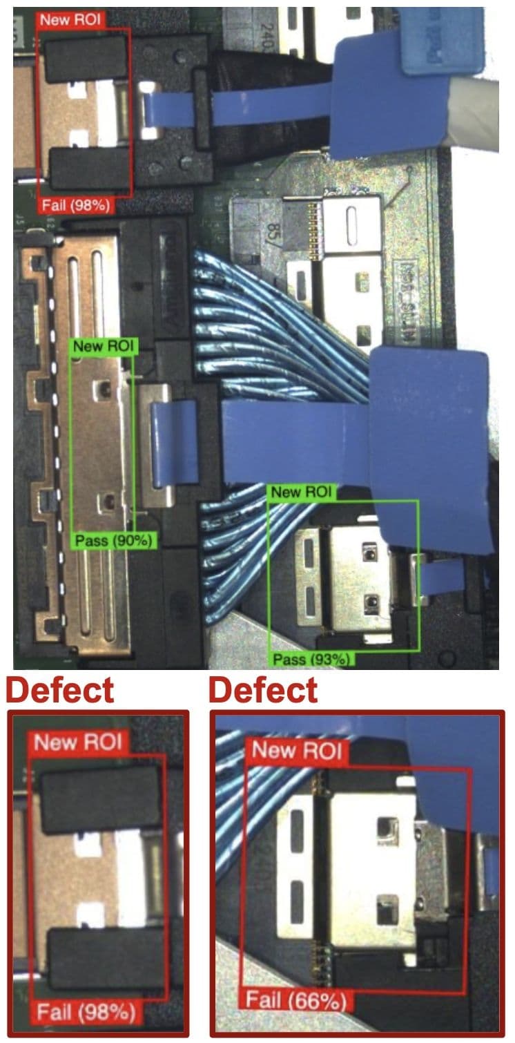
Connector & Pin Inspection
Eliminate bottlenecks from manual inspection. Our AI can instantly spot bent, missing, or contaminated pins inside high-density connectors and verify pin coplanarity to prevent connectivity failures.
Contamination & FOD Detection
Find foreign object debris, metal contaminants, and dust particles that threaten product reliability. Our vision system detects microscopic contamination that can cause short circuits or long-term degradation.
Semiconductor Packaging Inspection
Ensure perfect connections at the chip level. Verify wire bond placement and integrity on semiconductor packages, detecting broken or misplaced bonds. We inspect die attach quality for voids or excess material that affects thermal performance.
Final Assembly & Cosmetic Inspection
Guarantee a flawless customer experience. Find microscopic scratches, pits, and adhesive overflow on device housings, screens, and camera lenses, ensuring every product that ships is cosmetically perfect.
Our Impact in Connectors & Electronics

High Speed Connector Pin Defects
Multi-class defect detection on high-density automotive connectors
PCBA Soldering Defect Detection
AI-powered inspection of solder joints and component placement
Battery Laser Welding Defect Detection
Real-time laser weld inspection for EV battery packs
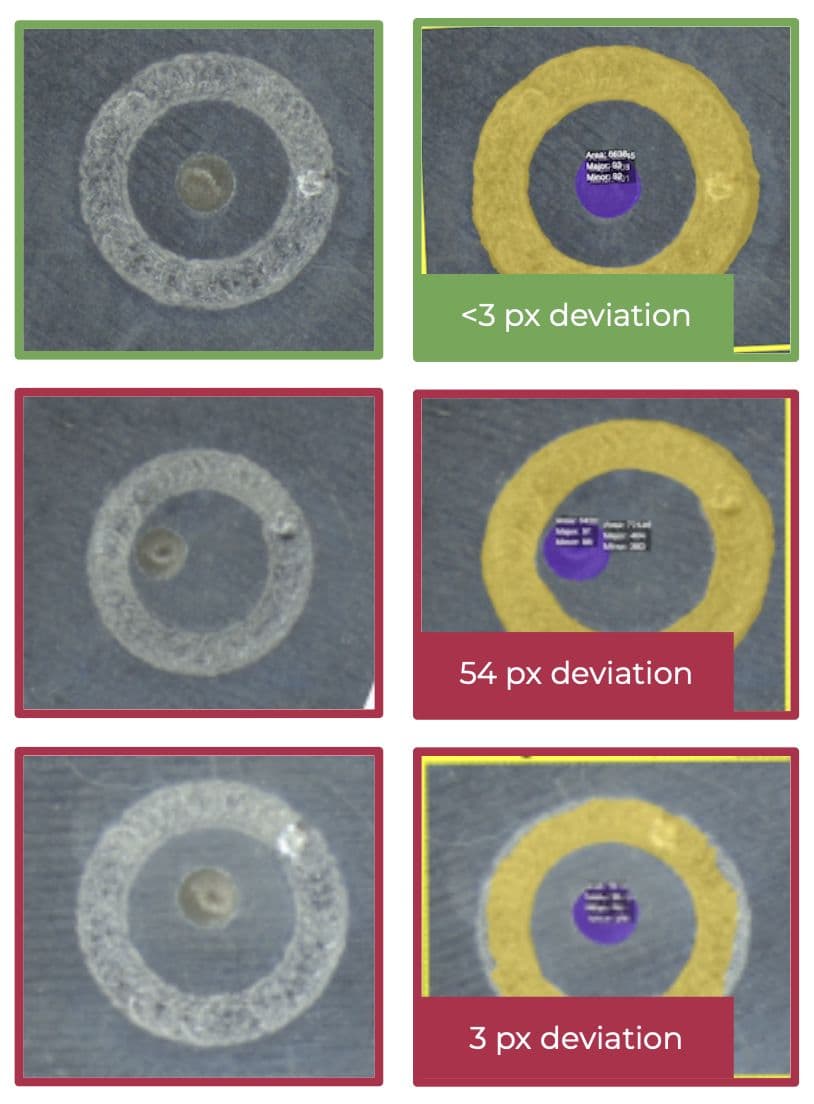
Connector Bent Pins Defect Case Study
Detecting minute bent pins and dust particles with telecentric lens
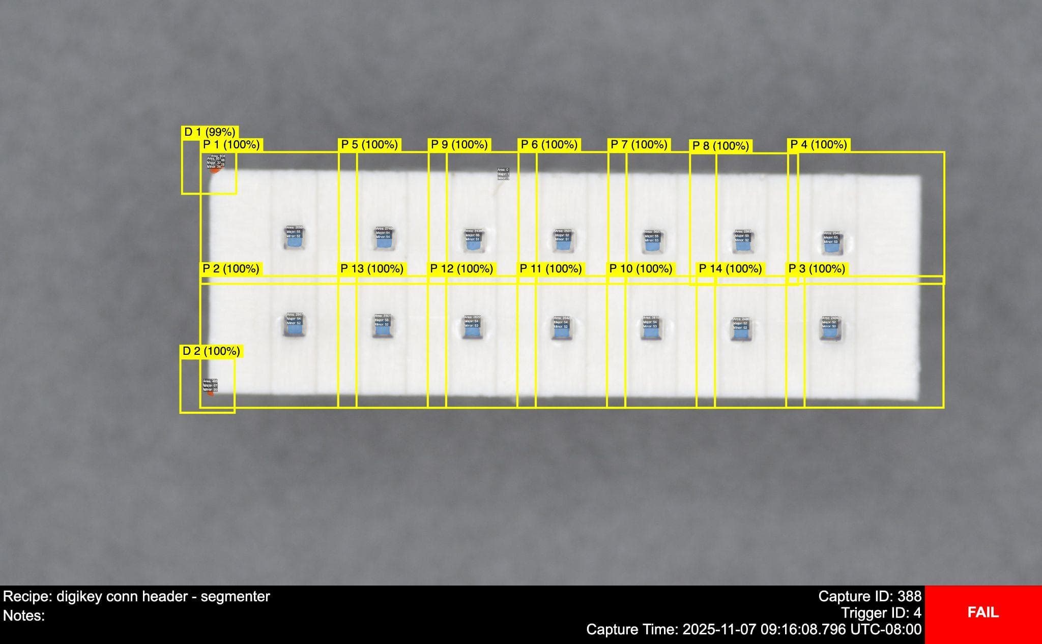
Electronics Connector Assembly Verification
Inspecting multiple soft-seated connectors in a single recipe
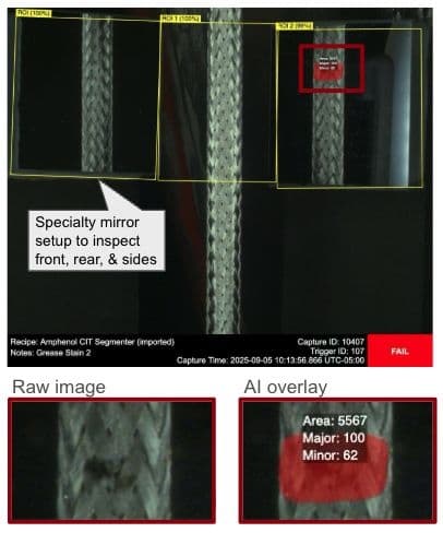
High Voltage Wire Braid Inspection
360° FOD and dent detection on high-voltage wire braids
Connector Inspection Applications

Bent Pin Inspection
Detect sub-degree angular deviations on high-density connector pins

Terminal Seating Verification
Verify every terminal is fully seated at the correct height

Housing Defect Detection
Catch cracks, flash, chips, and molding defects on housings

Debris & FOD Detection
Find foreign object debris inside connector cavities

Micro-Connector Inspection
Inspect fine-pitch connectors with sub-millimeter features

Multi-Variant Inspection
One AI system for dozens of connector variants

Laser Weld Inspection
Verify weld quality on terminal-to-wire connections

Hot Bar Soldering Inspection
Inspect FPC and fine-pitch solder joint quality

Conformal Coating Inspection
Verify coating coverage and keep-out zone cleanliness
Ready to Eliminate Connector Quality Escapes?
See how Overview AI can achieve 100% inspection coverage on your connector and electronics lines. Our team will analyze your specific applications and demonstrate what's possible.
Book a Demo