
Detecting Defects in Backplane Wafers with Air Gap Dielectric: A Machine Vision Walkthrough
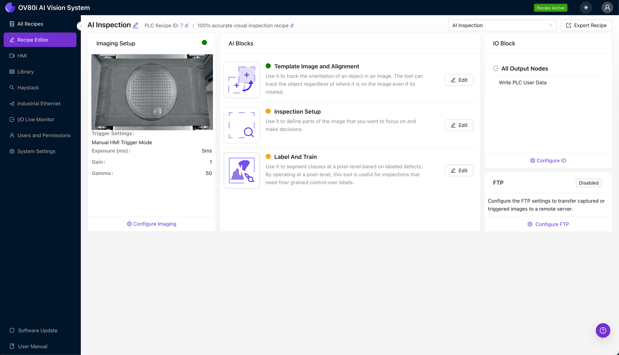
"Backplane wafers with air gap dielectric present unique inspection challenges due to sub-micron defects and subtle contrast variations. Machine vision with deep learning delivers consistent, objective inspection at full line speed—catching gap collapse, bridging, and contamination that human inspectors routinely miss."
The Problem: Why Air Gap Dielectric Inspection Challenges Even Experienced Teams
Backplane wafers with air gap dielectric architecture represent a critical advancement in reducing capacitance and signal crosstalk in high-performance semiconductor applications. However, the very properties that make air gaps effective—their delicate voids and precise geometries—also make them exceptionally difficult to inspect.
Common Defects in Air Gap Dielectric Structures
- Air gap collapse — partial or complete structural failure of the dielectric void
- Dielectric bridging — unintended material deposits connecting isolated regions
- Non-uniform gap spacing — variations in air gap dimensions affecting electrical performance
- Particle contamination — foreign debris trapped within the air gap cavity
- Delamination at interfaces — separation between the air gap structure and adjacent layers
- Pinhole formation — microscopic breaches in the supporting dielectric material
Human inspectors struggle with these defects because many occur at the sub-micron level and require consistent focus across thousands of inspection points. Fatigue sets in rapidly when examining repetitive wafer patterns, and the subtle contrast differences between acceptable and defective air gaps make reliable manual detection nearly impossible at production speeds.
The Solution: Machine Vision and Deep Learning
Machine vision systems equipped with deep learning algorithms excel precisely where human inspection fails. By training neural networks on labeled examples of both conforming and non-conforming air gap structures, these systems learn to recognize defect signatures that would escape even the most experienced human eye.
Overview.ai's approach delivers consistent, objective inspection at full line speed—eliminating the variability inherent in manual quality control. The OV80i system evaluates every wafer against the same learned criteria, ensuring that a defect detected on Monday morning receives the same classification on Friday afternoon.
Step 1: Imaging Setup
Begin by positioning the backplane wafer with air gap dielectric under the inspection camera, ensuring the wafer lies flat and the region of interest falls within the field of view. Proper staging is critical for capturing the subtle optical variations that indicate air gap integrity.
Navigate to "Configure Imaging" in the Overview.ai interface and adjust the Camera Settings. Fine-tune exposure time to reveal air gap boundaries without overexposing reflective metallization layers, and adjust gain to optimize signal-to-noise ratio for your specific dielectric stack.
Click "Save" to lock in your imaging parameters before proceeding.
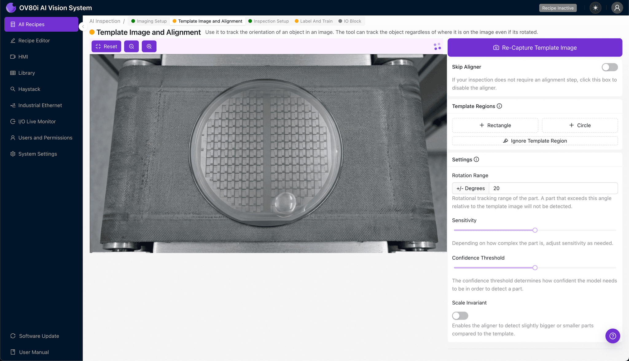
Step 2: Image Alignment
Navigate to "Template Image" and capture a reference image of a known-good wafer positioned in the standard orientation. This template serves as the baseline for automatic alignment of all subsequent inspection images.
Click "+ Rectangle" to add an alignment region around the main body of the inspection area—typically encompassing the active die region or a distinctive fiducial pattern. Set "Rotation Range" to 20 degrees to accommodate minor orientation variations during wafer handling without compromising alignment accuracy.
Step 3: Inspection Region Selection
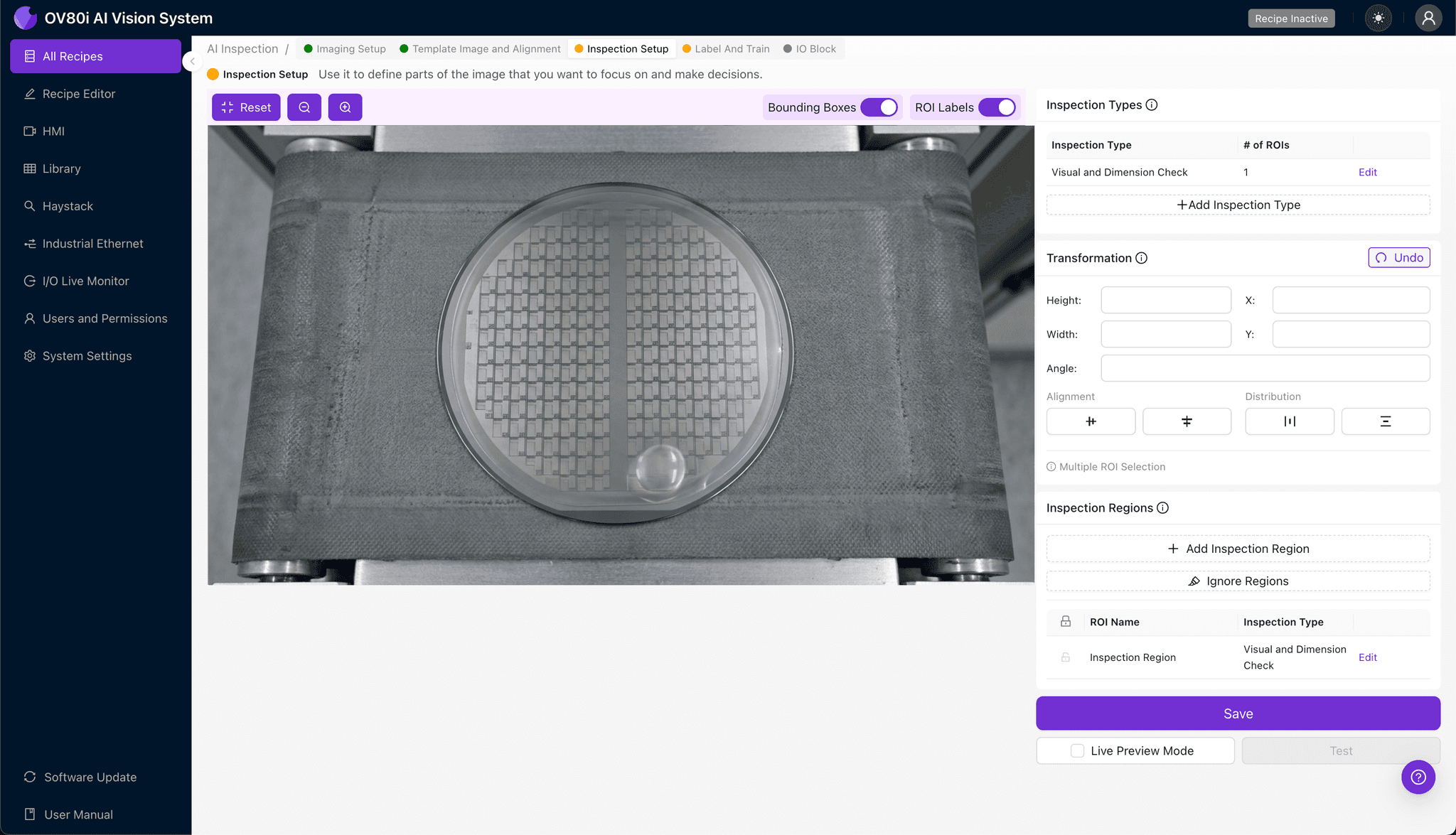
Navigate to "Inspection Setup" to define where the system should focus its analysis. Rename your "Inspection Types" to reflect the specific defect categories relevant to air gap structures—such as "Gap Collapse," "Contamination," or "Bridging."
Click "+ Add Inspection Region" for each critical area requiring evaluation. Resize the yellow bounding box to cover the air gap dielectric zones, interconnect regions, and layer interfaces where defects most commonly manifest.
Click "Save" to confirm your inspection configuration.
Step 4: Labeling Data
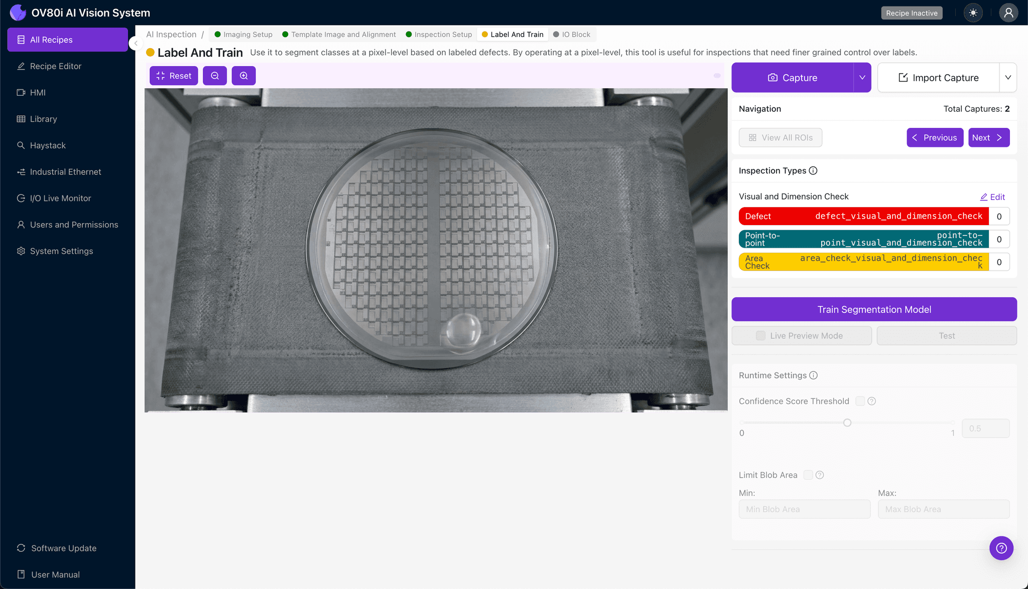
The human-in-the-loop labeling process is where your team's expertise trains the AI model. Review captured images and classify each as Good or Bad based on your quality standards and customer specifications.
Include representative samples across the full range of acceptable variation, as well as known failure modes from historical quality data. The more diverse and accurately labeled your training set, the more robust your deployed model will perform in production.
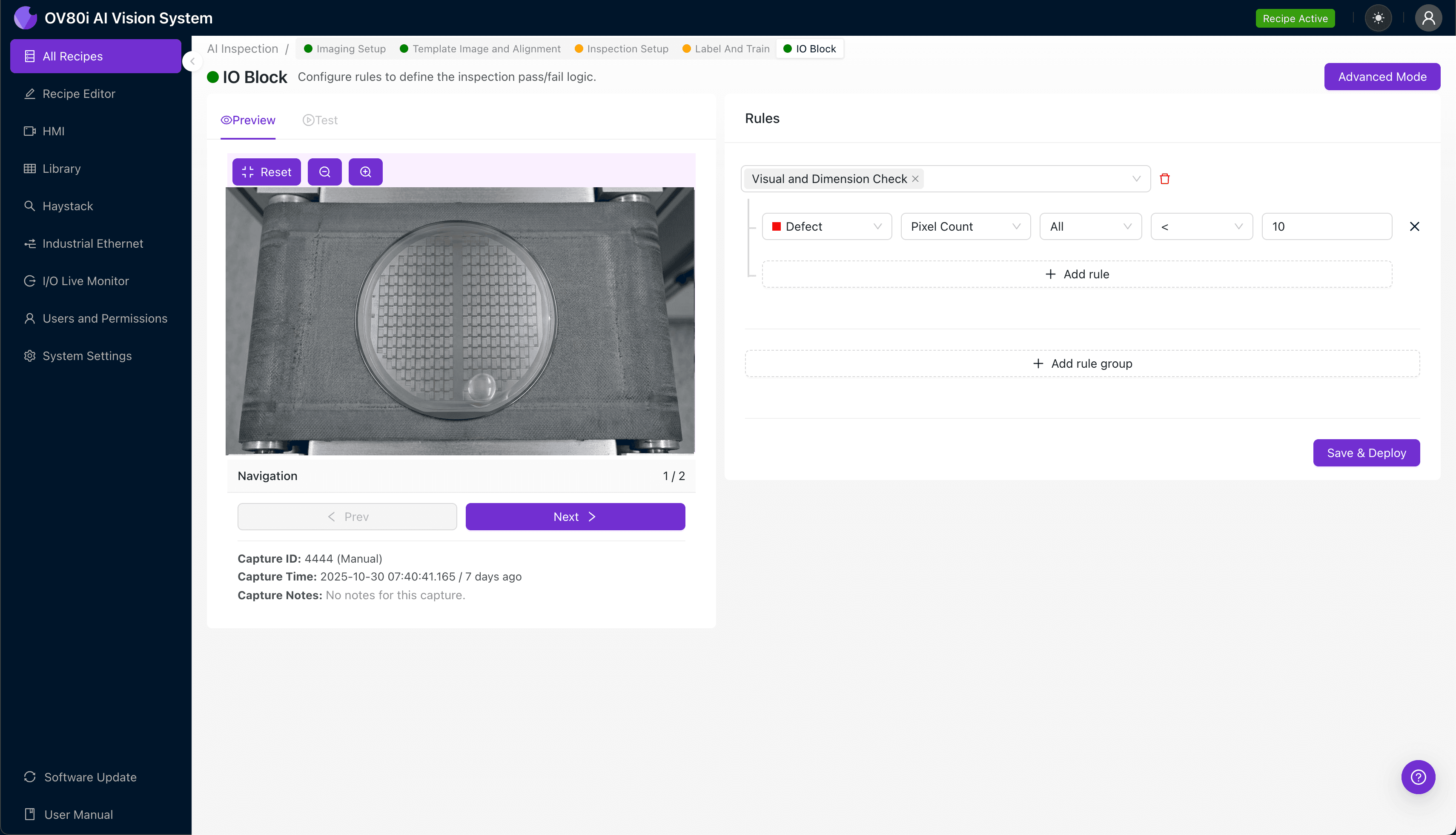
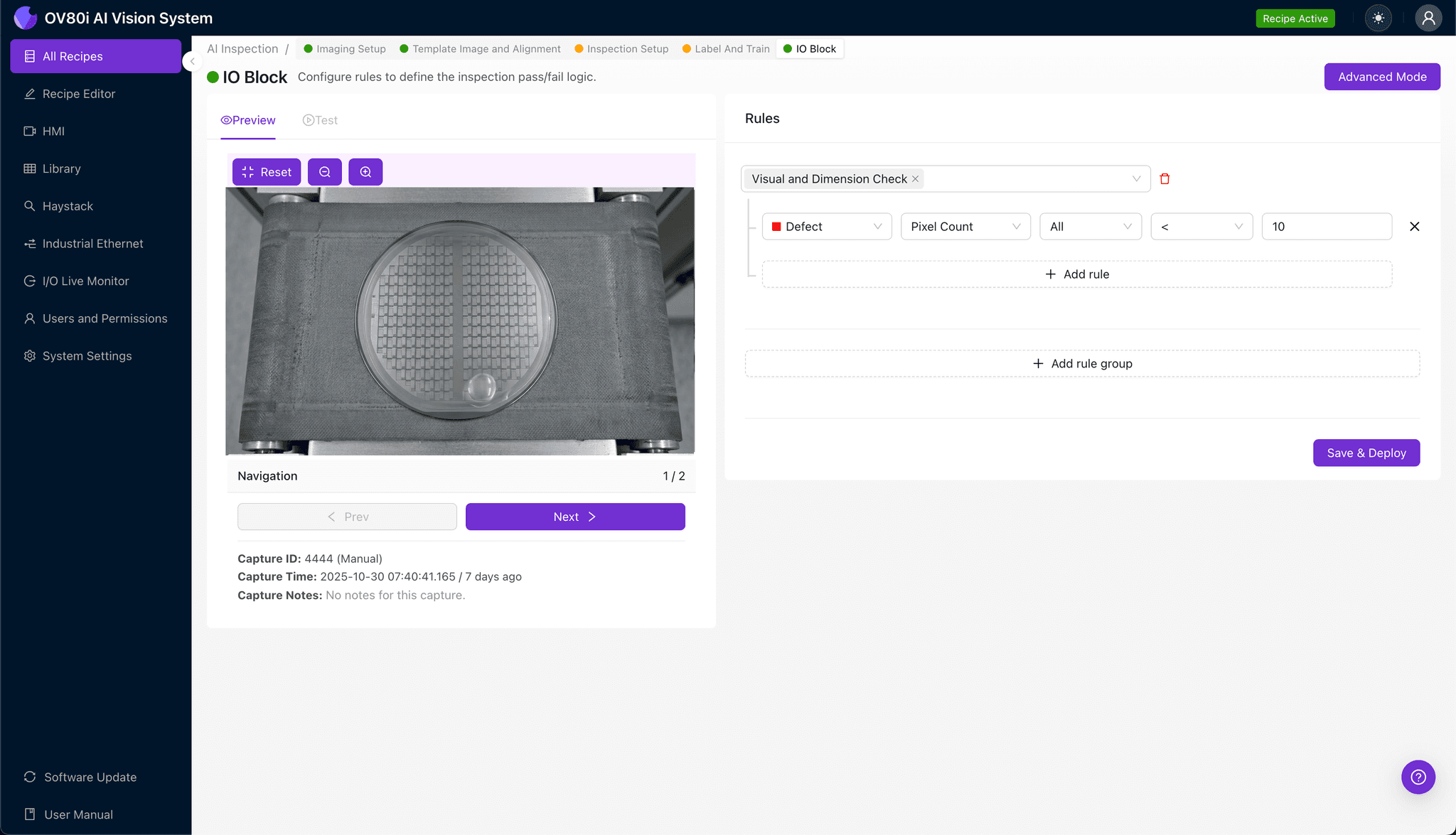
Step 5: Creating Rules
With your model trained, establish pass/fail logic based on the Inspection Types you defined earlier. Configure thresholds that align with your quality requirements—for example, rejecting any wafer showing gap collapse while flagging minor contamination for secondary review.
These rules gate automated acceptance directly on the production line, enabling real-time disposition decisions without manual intervention.
Key Outcomes & ROI
Implementing automated inspection for backplane wafers with air gap dielectric delivers measurable business impact:
- Reduced scrap rates — catch defects early before downstream processing adds cost to non-conforming material
- Higher throughput — inspect 100% of production at line speed without creating bottlenecks
- Enhanced compliance and traceability — maintain complete inspection records with timestamped images for audit and customer requirements
- Process improvement insights — identify defect trends and correlate with upstream process parameters to address root causes
Eliminate Inspection Blind Spots in Semiconductor Manufacturing
Stop relying on manual inspection for critical air gap dielectric quality control. Deploy Overview.ai to catch defects instantly at full production speed.