How to Inspect High-Speed Links with Thermal-Induced Skew Using AI-Powered Vision
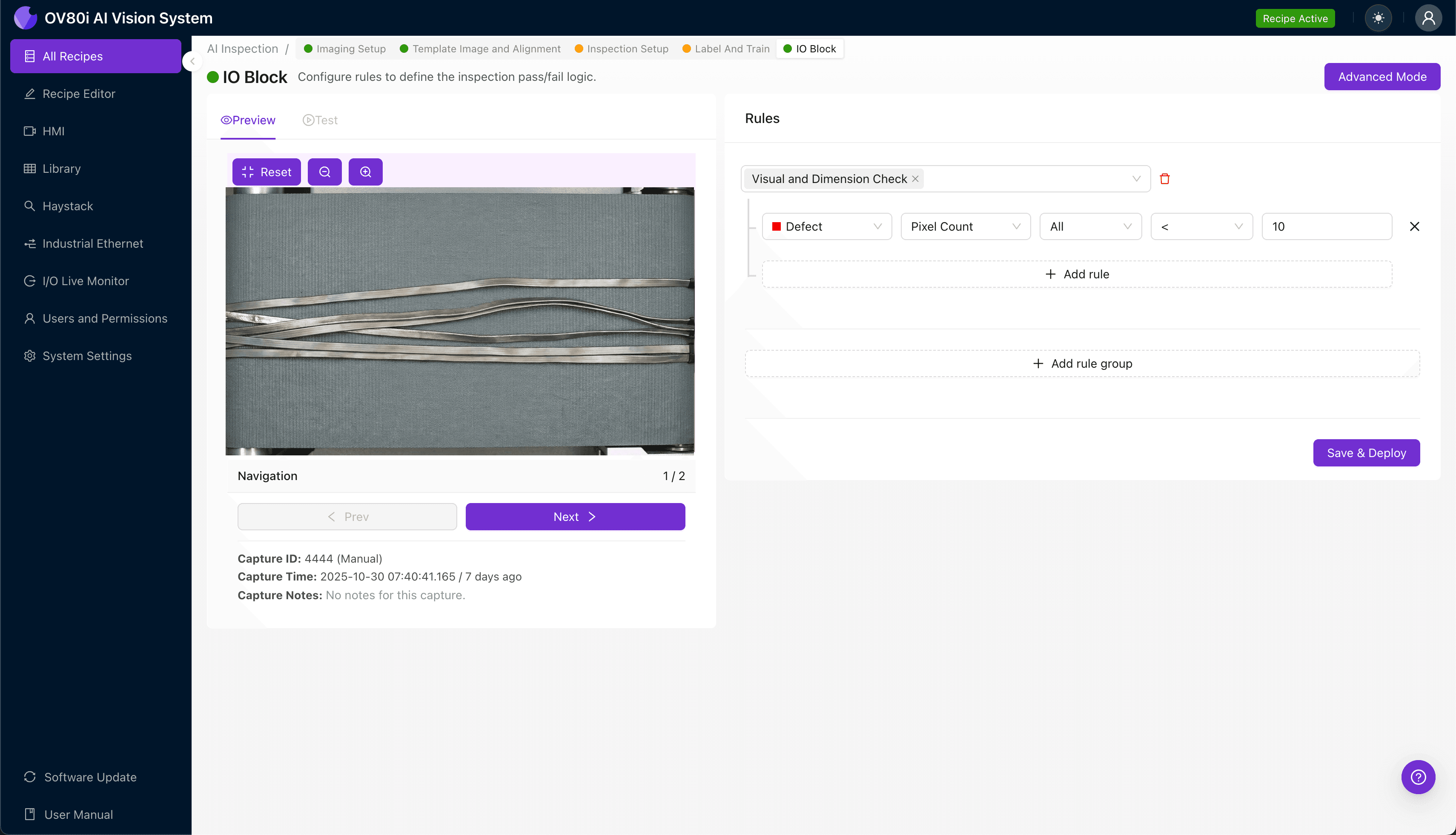
"Thermal-induced skew in high-speed links causes micro-level defects that devastate signal integrity. AI-powered visual inspection detects solder joint micro-fractures, trace warping, and delamination at full production speed—catching failures that human inspectors consistently miss."
The Problem: Why Thermal-Induced Skew Defects Slip Through
High-speed links are critical interconnects in data centers, telecommunications, and advanced electronics manufacturing. When thermal cycling causes differential expansion across signal pairs, the resulting skew can devastate signal integrity and cause catastrophic system failures.
Common defects in high-speed links with thermal-induced skew include:
- Differential pair length mismatch — uneven trace routing exacerbated by thermal stress
- Solder joint micro-fractures — hairline cracks at BGA or connector interfaces from thermal cycling
- Dielectric delamination — separation between PCB layers causing impedance discontinuities
- Copper trace warping — subtle bowing or lifting of signal traces under heat stress
- Connector pin misalignment — thermal expansion causing mechanical drift at interface points
- Via barrel cracking — stress fractures in plated through-holes affecting signal path continuity
Human inspectors struggle with these defects because many occur at the micron level and develop gradually over thermal cycles. Inspector fatigue compounds the problem—after hours of examining nearly identical components, consistency drops dramatically, and subtle skew-related anomalies escape detection.
The Solution: Machine Vision + Deep Learning
AI-powered visual inspection eliminates the variability inherent in manual quality control. Deep learning models trained on thousands of labeled images can detect subtle pattern deviations that indicate thermal-induced skew—even when those deviations are invisible to the human eye.
Overview.ai's approach delivers consistent, objective inspection at full line speed. The OV80i system captures high-resolution images, applies trained neural networks, and makes pass/fail decisions in milliseconds—enabling true 100% inline inspection without bottlenecking production.
Step 1: Imaging Setup
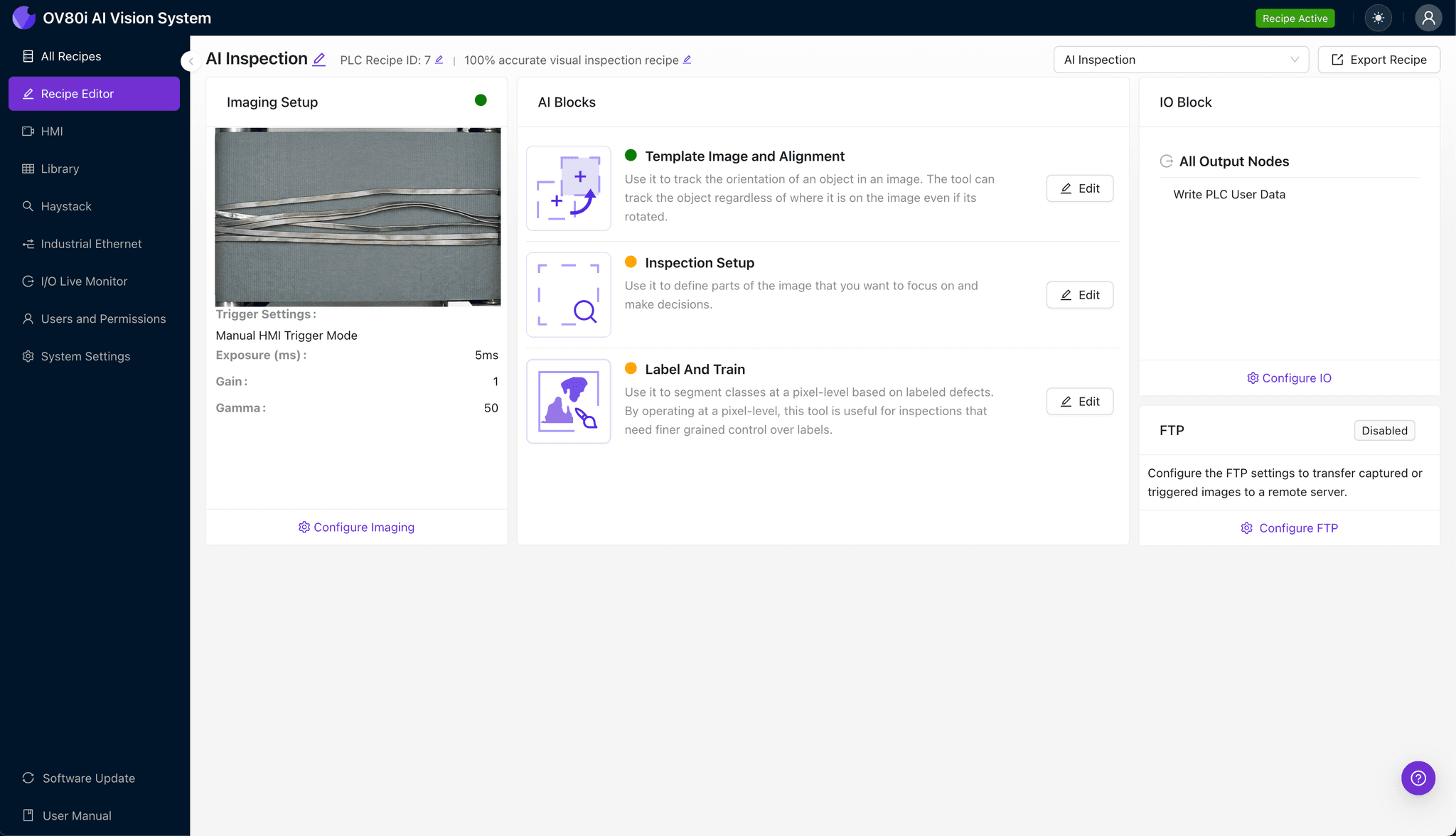
Position your high-speed link assembly under the OV80i camera, ensuring the component lies flat with all critical inspection areas visible. Proper lighting is essential—use diffuse illumination to minimize reflections on solder joints and connector surfaces.
Click "Configure Imaging" in the Overview interface to access Camera Settings. Adjust exposure to capture fine detail in solder joints without overexposing reflective surfaces, and tune gain to optimize signal-to-noise ratio for your specific link geometry.
Click "Save" once your image shows clear definition across all inspection zones.
Step 2: Image Alignment
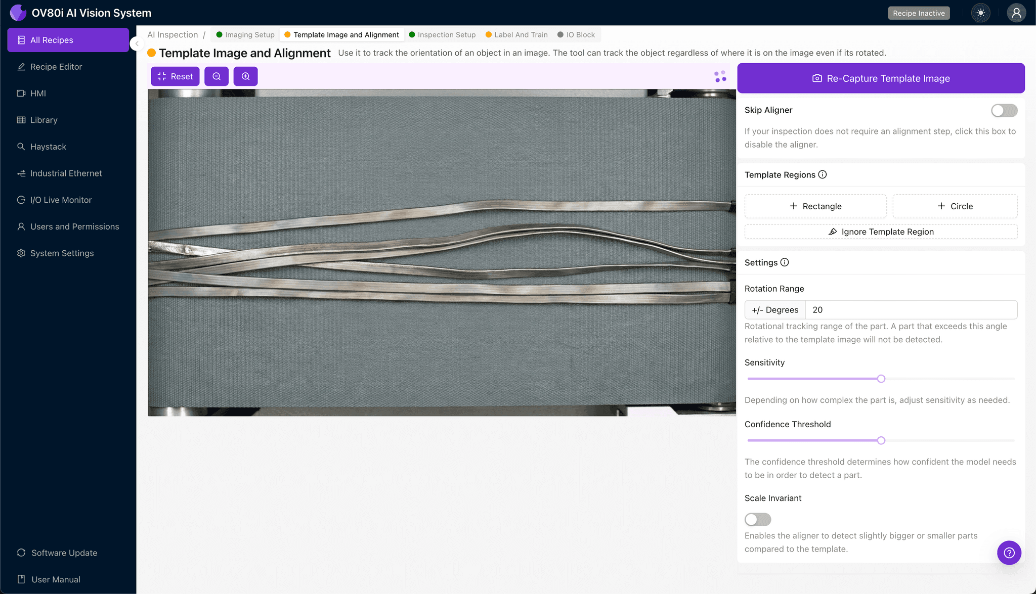
Navigate to the "Template Image" tab and capture a reference image of a known-good high-speed link. This template anchors all future inspections, ensuring consistent positioning regardless of minor placement variations on the line.
Click "+ Rectangle" and draw a region around the main connector body or PCB edge—this gives the alignment algorithm a stable reference feature. Set "Rotation Range" to 20 degrees to accommodate typical placement variability while maintaining accurate defect localization.
Step 3: Inspection Region Selection
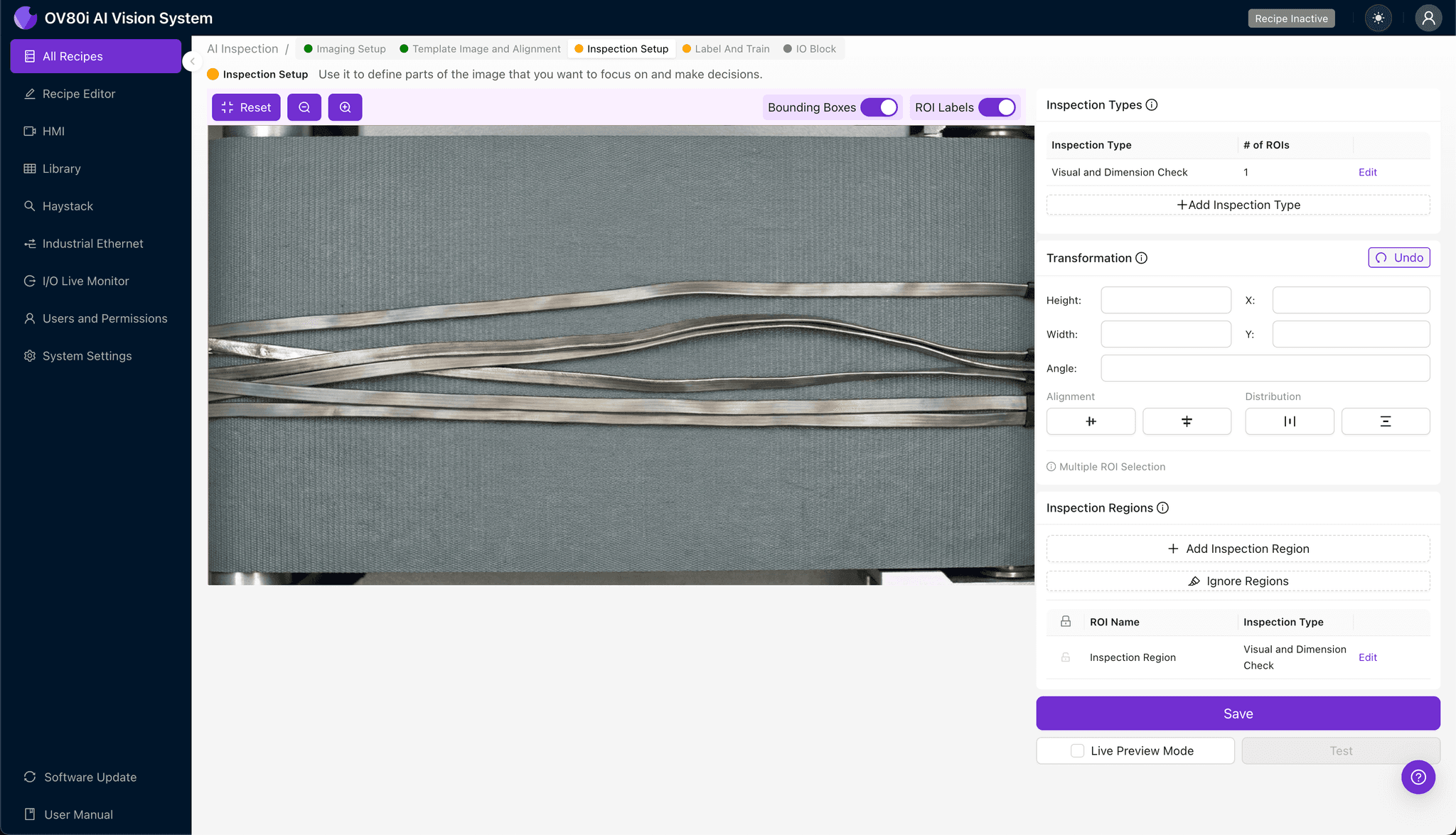
Navigate to "Inspection Setup" to define where the system should look for defects. Rename your "Inspection Types" with descriptive labels like "Solder_Joint_Integrity," "Trace_Alignment," or "Connector_Pin_Position."
Click "+ Add Inspection Region" for each critical area. Resize the yellow bounding box to cover specific zones: differential pair traces, connector interfaces, via arrays, and any areas prone to thermal stress concentration.
Click "Save" after defining all regions.
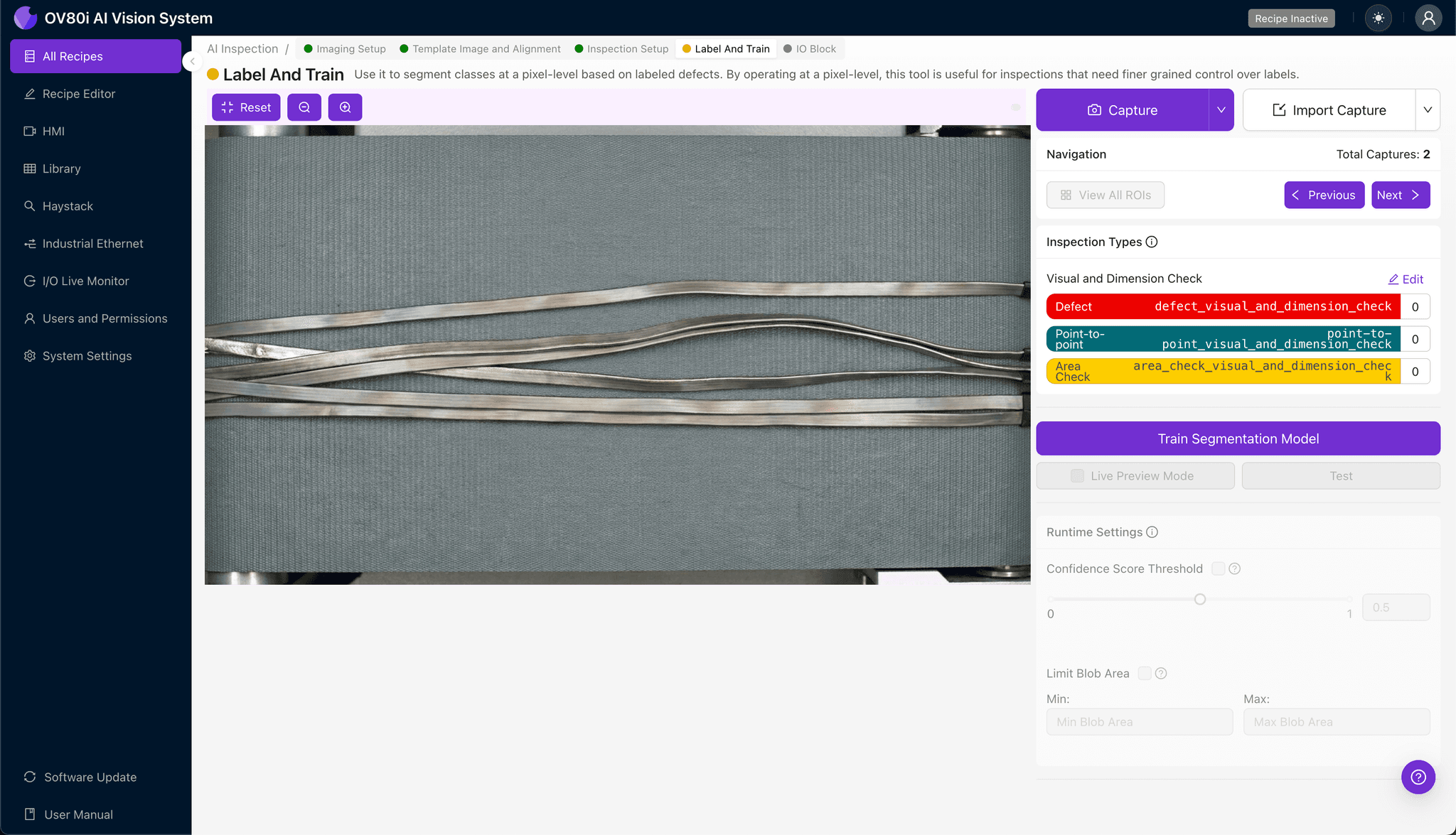
Step 4: Labeling Data
This human-in-the-loop phase teaches the AI what constitutes acceptable vs. defective parts. Review captured images and label each as Good or Bad based on your quality specifications.
Include representative samples across your full production variation—different lot codes, ambient temperatures, and assembly shifts. Most importantly, incorporate known failure modes: links that failed in-field testing, customer returns, and any documented thermal-induced skew incidents.
The more diverse your labeled dataset, the more robust your trained model becomes.
Step 5: Creating Rules
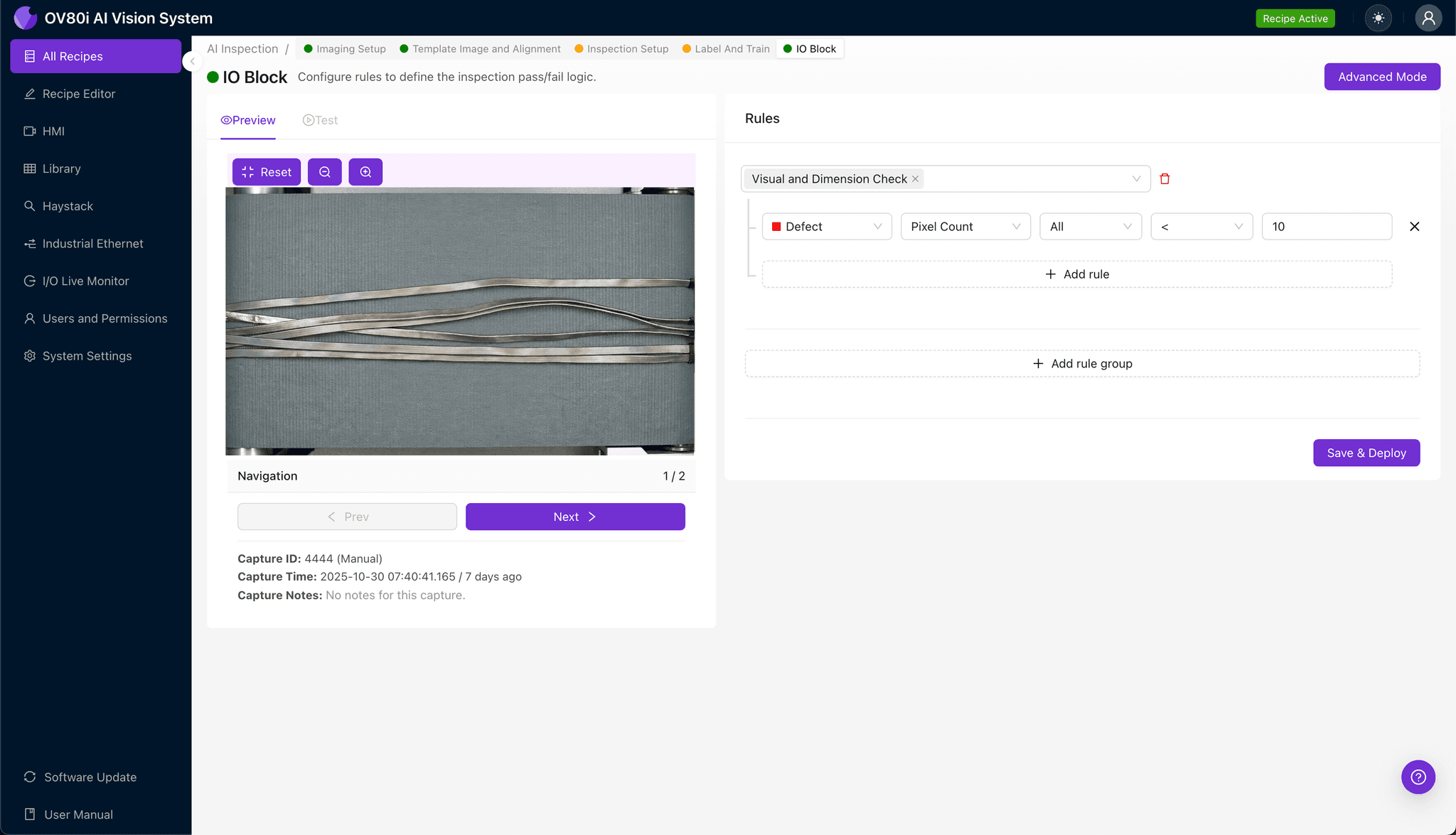
Configure your pass/fail logic based on the Inspection Types you defined earlier. For example, set rules that flag any component where "Solder_Joint_Integrity" scores below your confidence threshold or where multiple regions show marginal results simultaneously.
These rules gate automated acceptance on your production line. Parts that pass proceed automatically; flagged units route to secondary inspection or rejection bins—all without operator intervention.
Key Outcomes & ROI
Implementing AI-powered inspection for high-speed links with thermal-induced skew delivers measurable business impact:
- Reduced scrap rates — catch defects before additional value-add processing
- Higher throughput — inspect 100% of units without creating bottlenecks
- Compliance and traceability — maintain complete inspection records for automotive, aerospace, or telecom certifications
- Process improvement insights — analyze defect trends to identify upstream issues like thermal profile problems or supplier material variations
Eliminate Thermal Skew Defects Today
Stop relying on manual inspection for critical high-speed links. Deploy Overview.ai to catch thermal-induced skew defects instantly—before they reach your customers.