Optical Waveguide Inspection: Detecting Scattering Loss from Surface Roughness with AI-Powered Vision
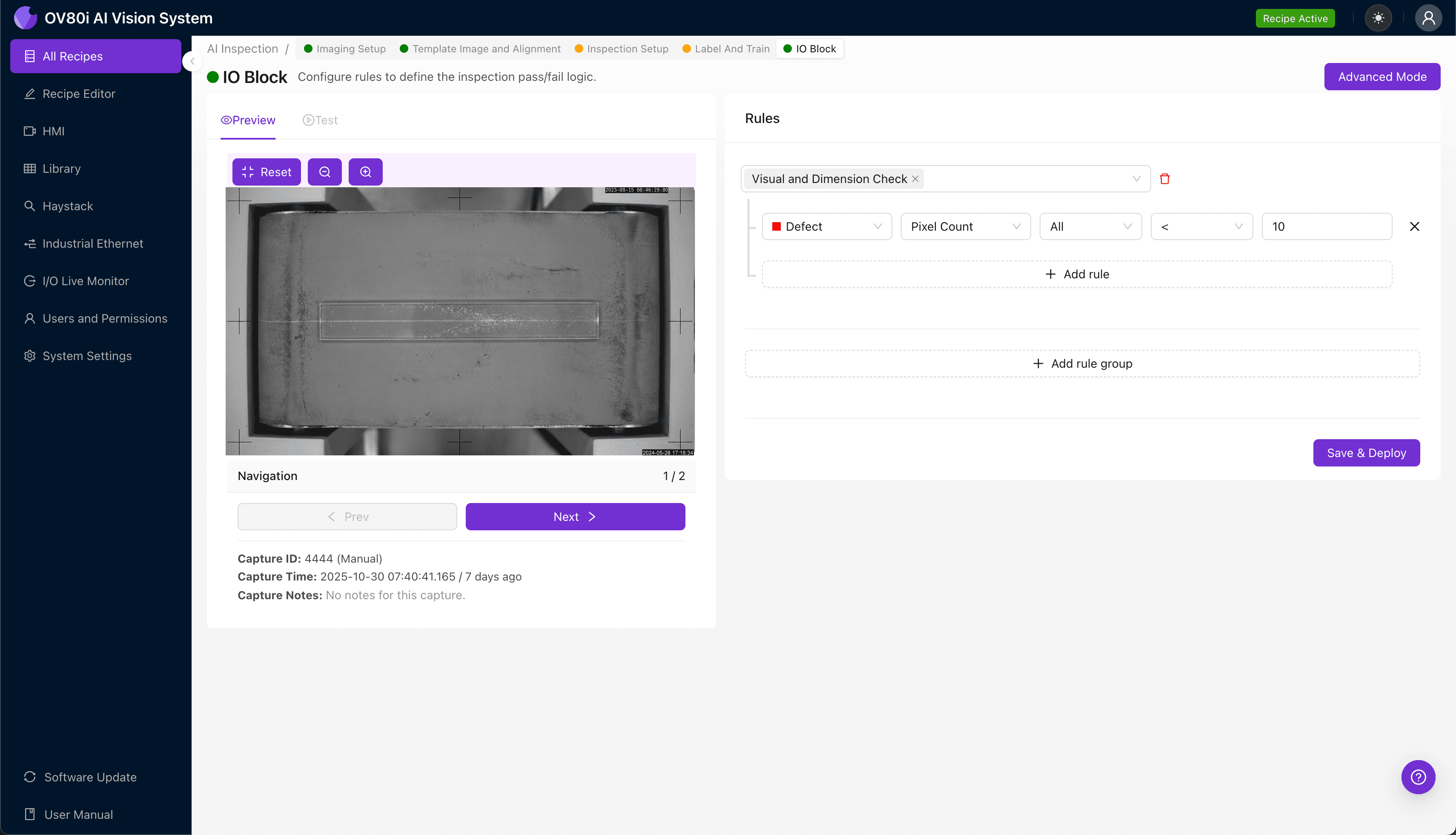
"Nanometer-scale surface roughness in optical waveguides causes significant scattering losses that degrade signal integrity. Overview.ai's deep learning-powered inspection detects these critical defects consistently at production speed, protecting yield and device performance in demanding photonics applications."
The Problem: Why Surface Roughness Defects Threaten Waveguide Performance
Optical waveguides are the backbone of modern photonic devices, fiber optic communications, and integrated optical circuits. Even nanometer-scale surface imperfections can cause significant scattering losses, degrading signal integrity and rendering components unusable.
Common Defects in Optical Waveguide Manufacturing
- Sidewall roughness — Irregularities along the waveguide edges that scatter light perpendicular to the propagation direction
- Core-cladding interface defects — Boundary imperfections between the core and cladding layers causing modal dispersion
- Surface pitting — Microscopic voids or depressions from etching processes that create localized scattering centers
- Contamination particles — Sub-micron debris embedded during deposition that disrupts optical transmission
- Delamination zones — Areas where thin-film layers separate, creating refractive index discontinuities
- Etch residue striations — Periodic patterns left by plasma or wet etching that introduce systematic losses
Manual inspection of optical waveguides presents significant challenges due to the microscopic scale of critical defects. Human inspectors experience rapid fatigue when examining features measured in nanometers, leading to inconsistent quality gates and escaped defects that only surface during final device testing.
The Solution: Machine Vision and Deep Learning for Waveguide Quality Control
Traditional rule-based vision systems struggle with optical waveguide inspection because scattering-inducing roughness varies widely in appearance and severity. Deep learning models excel here—they learn the subtle visual signatures of roughness patterns that correlate with unacceptable scattering loss, even when those patterns would be invisible to conventional algorithms.
Overview.ai's approach delivers consistent, objective inspection at production line speeds. By training neural networks on labeled examples of acceptable and defective waveguides, the system develops an understanding of quality that matches—and often exceeds—expert human judgment, while maintaining 100% inspection coverage without fatigue or drift.
Step 1: Imaging Setup
Position the optical waveguide sample under the camera, ensuring the inspection surface faces the lens with consistent orientation. Proper lighting is critical—consider using darkfield or differential interference contrast illumination to highlight surface roughness features.
Navigate to "Configure Imaging" in the software interface. Adjust Camera Settings including exposure time and gain to maximize contrast on roughness features while avoiding saturation on reflective waveguide surfaces.
Click "Save" to lock in your imaging parameters.
Step 2: Image Alignment
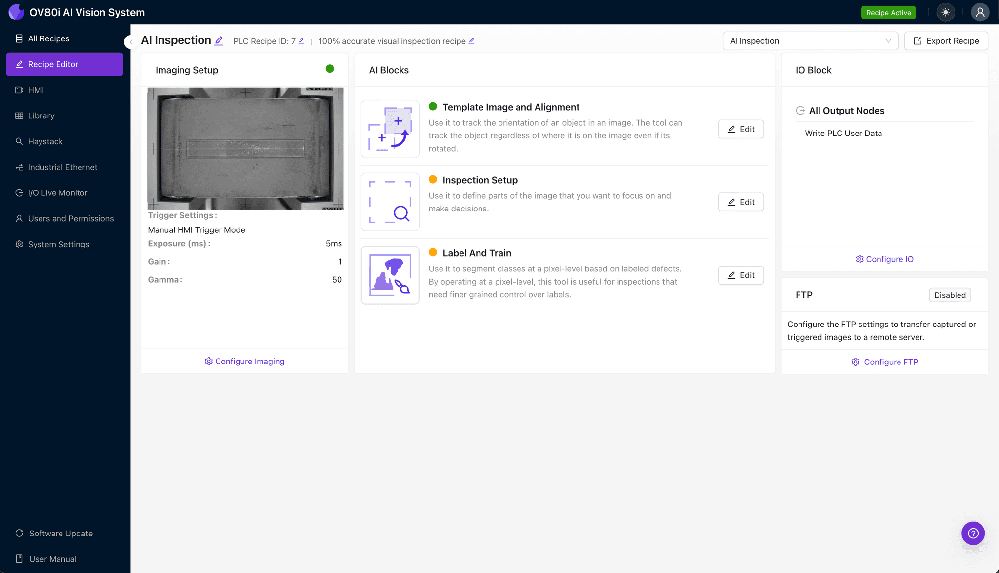
Navigate to "Template Image" to establish a reference for part alignment. Capture a Template image of a correctly positioned waveguide that represents your standard orientation.
Click "+ Rectangle" to add an alignment region around the main waveguide body or fiducial markers. Set "Rotation Range" to 20 degrees to accommodate minor orientation variations during automated handling.
Step 3: Inspection Region Selection
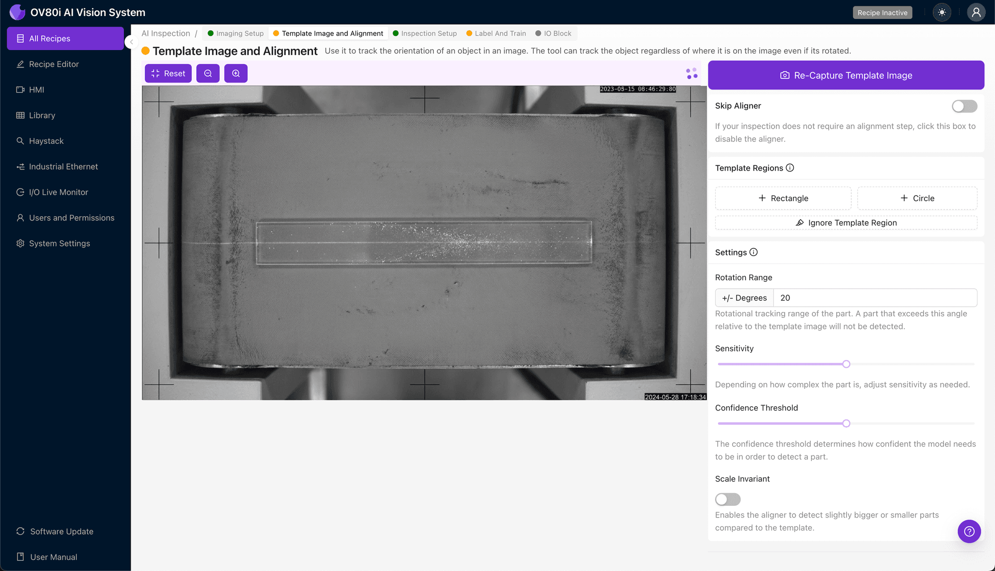
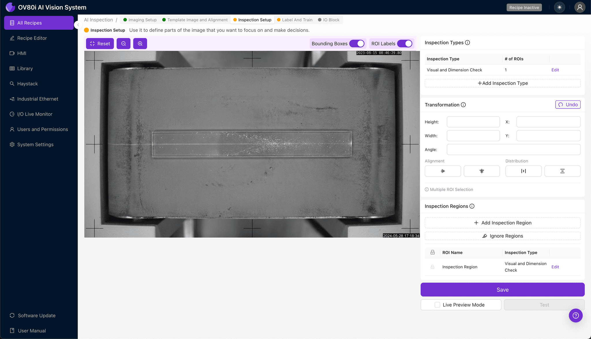
Navigate to "Inspection Setup" to define where the system should look for defects. Rename your "Inspection Types" to reflect waveguide-specific categories such as "Sidewall Roughness," "Surface Contamination," and "Interface Defects."
Click "+ Add Inspection Region" for each critical area. Resize the yellow bounding box to cover sidewall edges, core surfaces, and transition zones where roughness most commonly occurs.
Click "Save" to confirm your inspection regions.
Step 4: Labeling Data
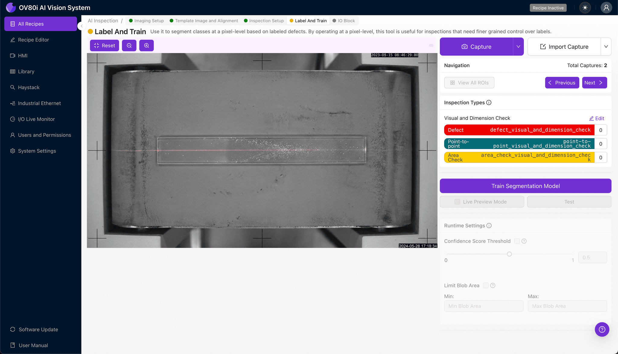
The human-in-the-loop labeling process is where your domain expertise trains the AI. Review captured images and label each as Good (acceptable scattering loss) or Bad (excessive roughness).
Include representative samples across your full production variation—different batches, equipment states, and environmental conditions. Ensure known failure modes are well-represented so the model learns to catch the defects that matter most to downstream performance.
Step 5: Creating Rules
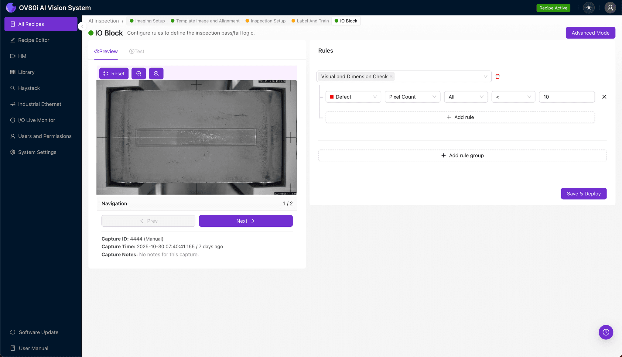
Configure pass/fail logic based on your defined Inspection Types. You might require all regions to pass, or allow minor roughness in non-critical zones while enforcing strict standards on primary optical paths.
These rules gate automated acceptance on the production line, ensuring only waveguides meeting your scattering loss specifications proceed to packaging or integration.
Key Outcomes & ROI
Implementing AI-powered visual inspection for optical waveguide roughness delivers measurable business impact:
- Reduced scrap rates — Catch defects earlier in production before additional value-added processing
- Higher throughput — Eliminate inspection bottlenecks with automated 100% inline screening
- Compliance and traceability — Maintain complete inspection records for quality audits and customer documentation requirements
- Process improvement insights — Correlate defect trends with upstream equipment or process parameters to address root causes
Conclusion
Surface roughness in optical waveguides directly impacts scattering loss and device performance. With Overview.ai's deep learning-powered inspection, manufacturers can detect these critical defects consistently, objectively, and at production speed—protecting both yield and reputation in demanding photonics markets.
Eliminate Waveguide Defects Today
Stop relying on manual inspection for nanometer-scale roughness. Deploy Overview.ai to catch scattering loss defects instantly.