Detecting Contaminated Grating Couplers on Photonic ICs: A Machine Vision Walkthrough
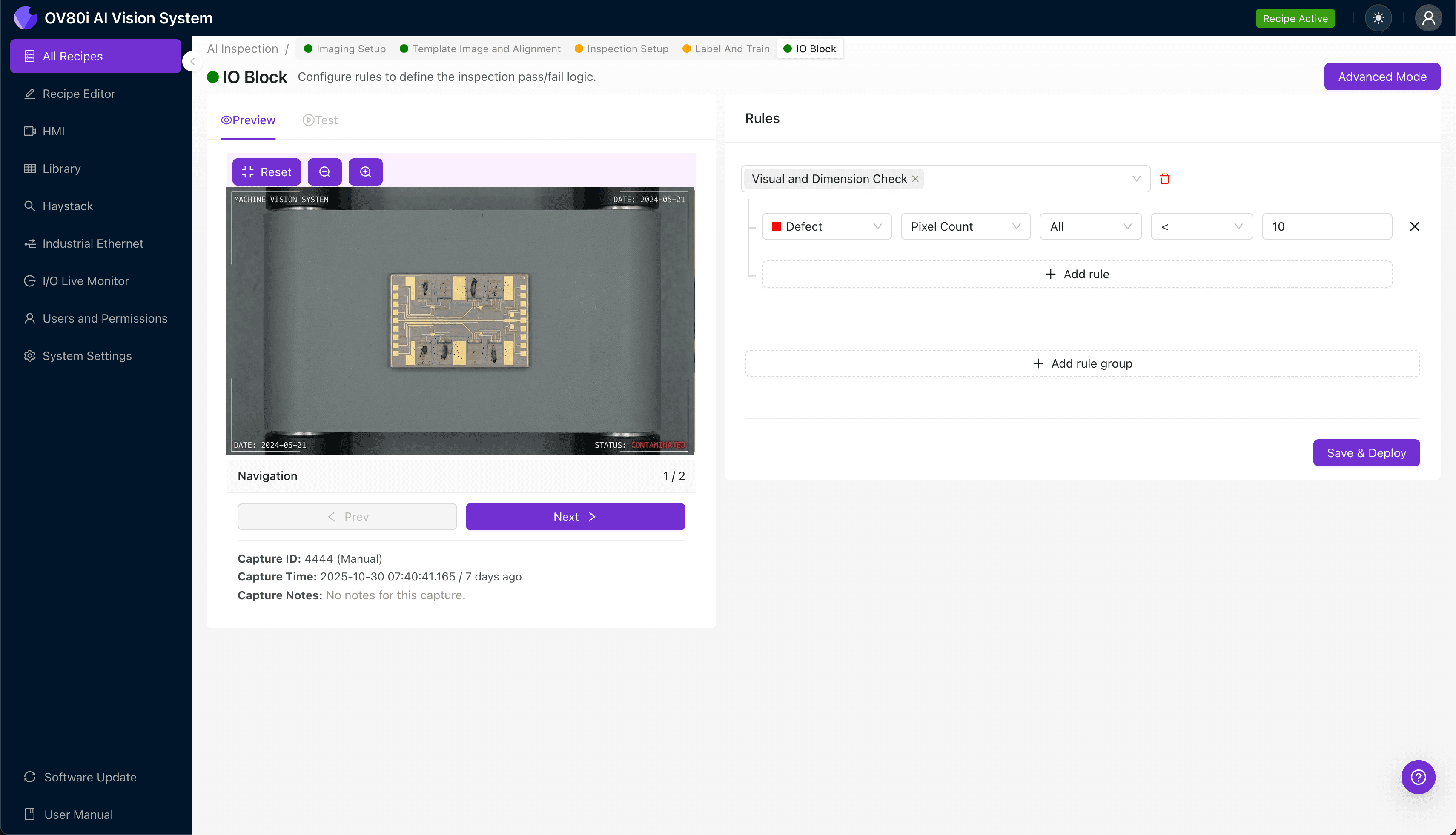
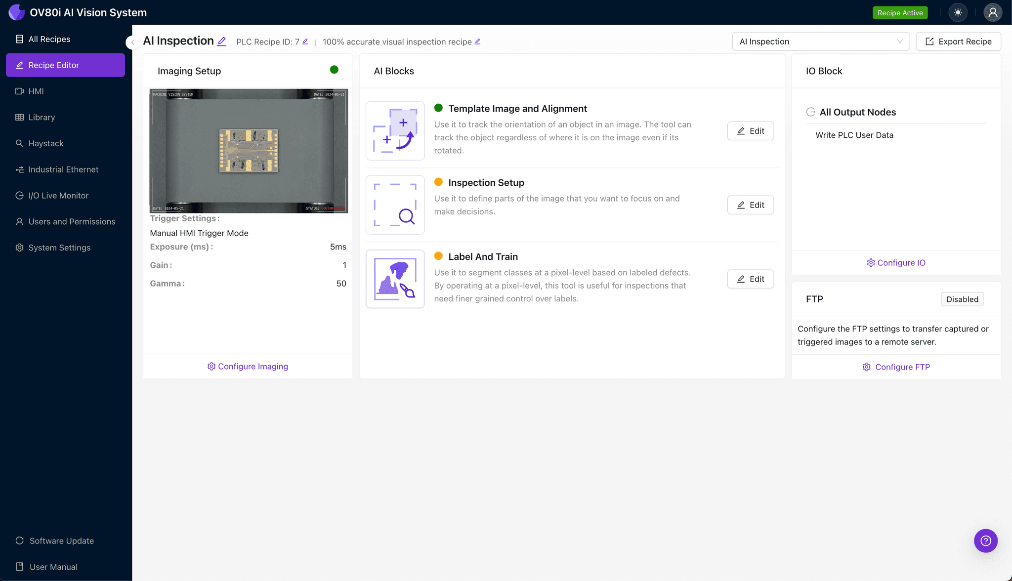
"Grating couplers are the critical optical interface on PICs, and even nanoscale contamination can cause catastrophic signal loss. Overview.ai's deep learning platform transforms this challenging inspection into a reliable, automated process that catches defects human inspectors consistently miss."
The Problem: Why Contaminated Grating Couplers Slip Through Manual Inspection
Grating couplers are the critical optical interface on Photonic Integrated Circuits (PICs), enabling light to enter and exit the chip with precision. Even nanoscale contamination on these structures can cause catastrophic signal loss, making detection essential before devices ship to customers.
Common Defects Found on Contaminated Grating Couplers:
- Particulate contamination – Dust, debris, or process residue lodged between grating lines
- Organic film residue – Thin chemical films from incomplete cleaning or outgassing
- Scratches across grating teeth – Handling damage that disrupts the periodic structure
- Etching residue buildup – Polymer or photoresist remnants from fabrication
- Metal flake deposition – Microscopic metallic particles from equipment wear
- Moisture-induced haze – Water spots or condensation marks affecting optical clarity
Human inspectors struggle with grating coupler inspection due to the microscopic scale of defects and the repetitive, high-concentration nature of the task. Fatigue sets in quickly when examining hundreds of identical structures, and subtle contamination variations are easily missed under time pressure.
The Solution: Machine Vision and Deep Learning for Consistent Detection
Traditional rule-based machine vision systems often fail on grating coupler inspection because contamination appears in unpredictable forms, locations, and optical signatures. Deep learning models, however, learn to recognize the subtle visual patterns that distinguish clean couplers from contaminated ones—even when defects don't follow predictable rules.
Overview.ai's approach delivers consistent, objective inspection at line speed, eliminating the variability inherent in human judgment. The system doesn't get tired, doesn't rush at the end of a shift, and flags the same defect the same way every single time.
Step 1: Imaging Setup
Position the PIC wafer or die under the OV80i's high-resolution camera, ensuring the grating coupler region is within the field of view. Proper lighting angle is critical—contamination often reveals itself through scatter or shadow effects that require optimized illumination.
Navigate to "Configure Imaging" in the Overview.ai interface. Adjust Camera Settings including exposure time and gain to maximize contrast between the grating structure and any surface contamination.
Click "Save" to lock in your imaging parameters.
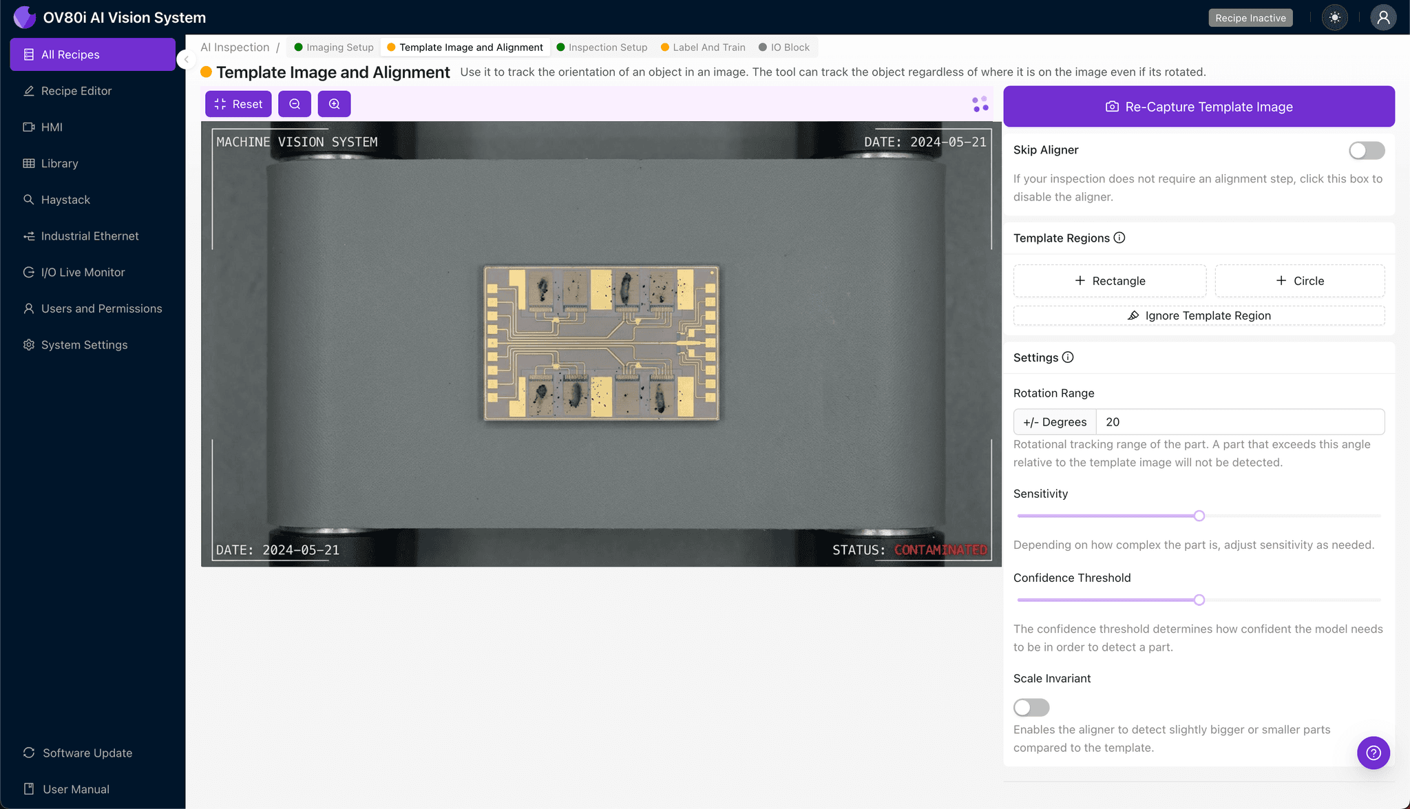
Step 2: Image Alignment
Navigate to the "Template Image" tab and capture a reference image of a known-good PIC. This template ensures consistent positioning across all inspected units, even when parts arrive at slightly different orientations.
Click "+ Rectangle" to draw an alignment region around the main body of the PIC or a distinctive fiducial feature. Set the "Rotation Range" to 20 degrees to accommodate expected positional variation on the line.
Step 3: Inspection Region Selection
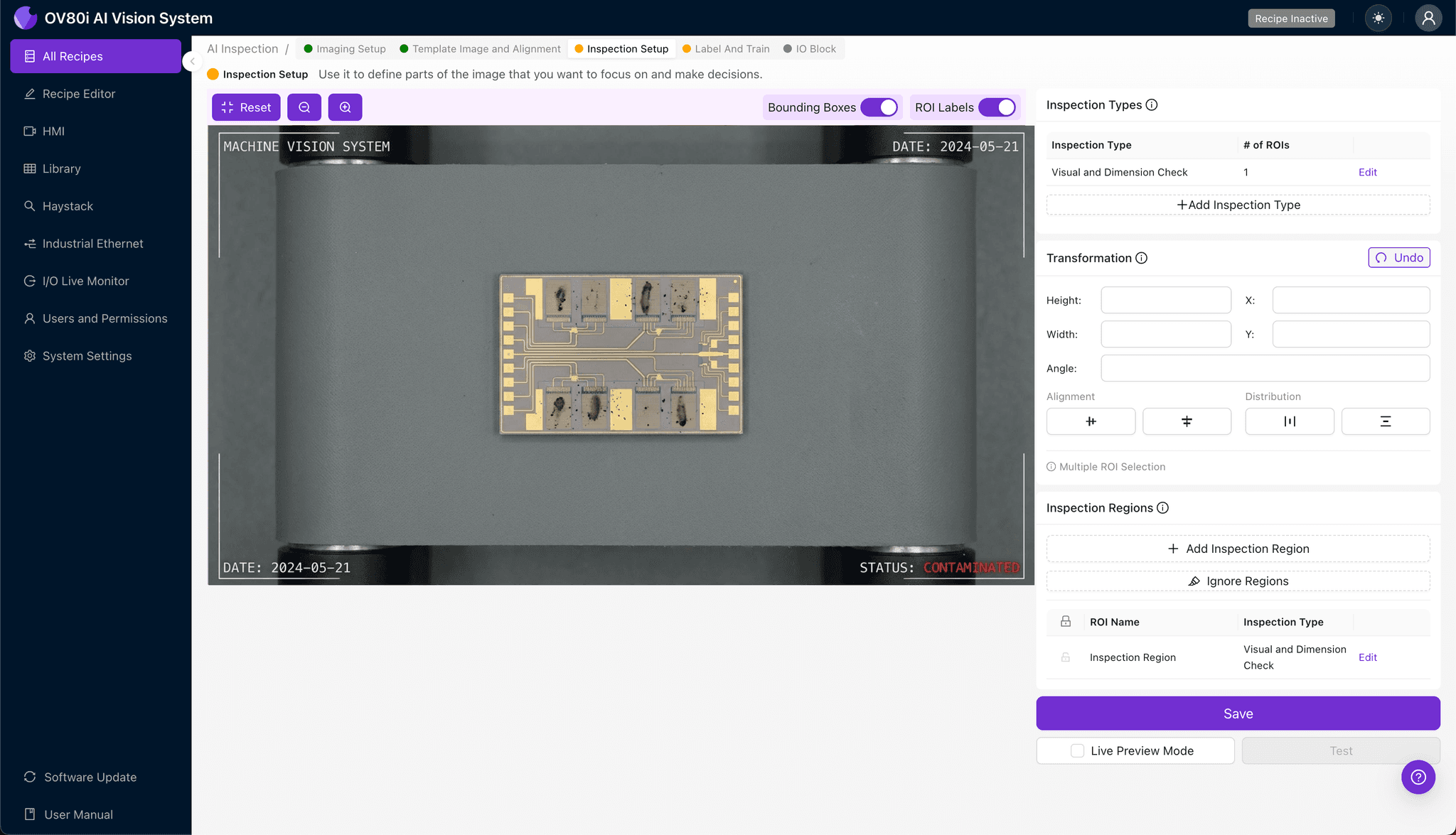
Navigate to "Inspection Setup" from the main menu. Rename your "Inspection Types" to reflect the specific defect categories—for example, "Grating Contamination" or "Coupler Surface Defects."
Click "+ Add Inspection Region" to define where the system should focus its analysis. Resize the yellow bounding box to cover the critical grating coupler area, ensuring all coupling teeth and the surrounding substrate are included.
Click "Save" to confirm your inspection zones.
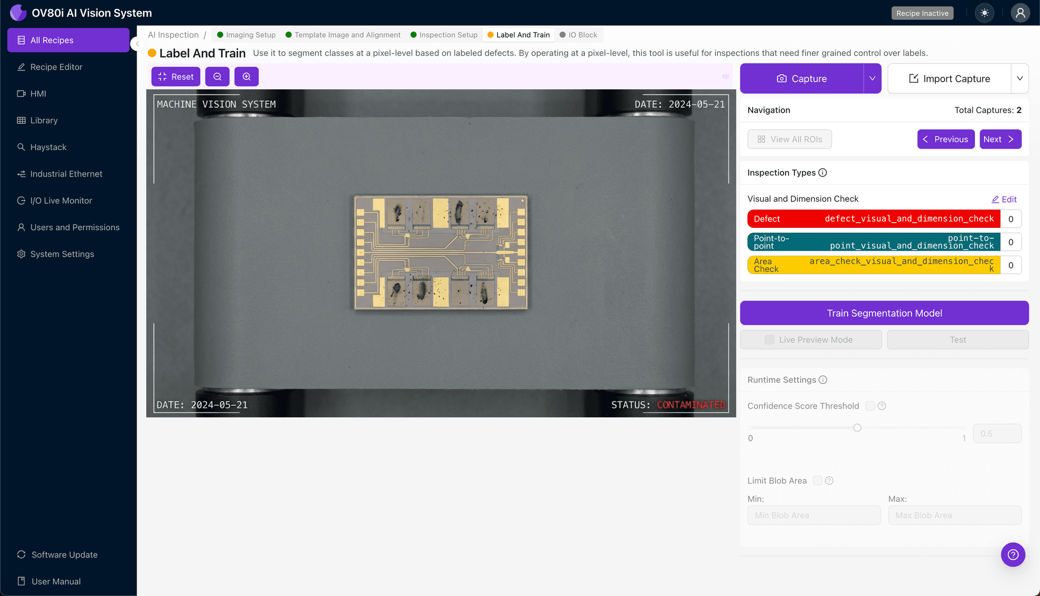
Step 4: Labeling Data
This is where human expertise trains the AI. Inspectors review captured images and label each grating coupler as Good (acceptable) or Bad (contaminated/defective).
Include representative samples across all contamination types—particulates, films, scratches, and residue. The model learns best when it sees the full range of known failure modes and borderline cases that define your quality threshold.
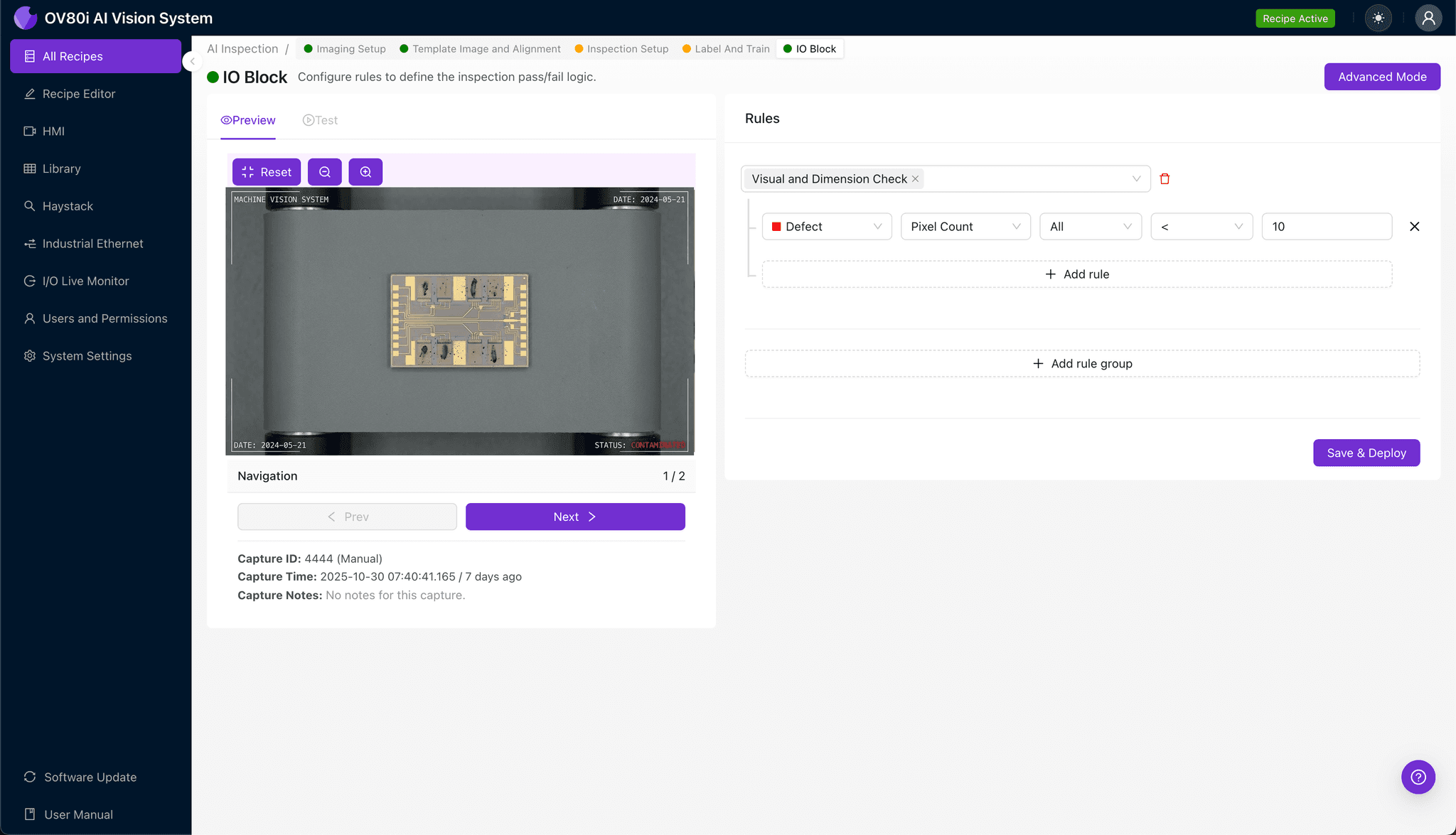
Step 5: Creating Rules
Define your pass/fail logic based on the Inspection Types you've configured. For example, any detection of "Grating Contamination" above a confidence threshold triggers automatic rejection.
These rules gate automated acceptance on the production line, ensuring only PICs meeting your quality standard proceed to packaging or further assembly.
Key Outcomes & ROI
Implementing AI-powered inspection for grating coupler contamination delivers measurable business impact:
- Reduced scrap rates – Catch contamination early before value-added processing compounds losses
- Higher throughput – Inspect 100% of units at line speed without creating bottlenecks
- Compliance and traceability – Maintain complete inspection records with timestamped images for customer audits
- Process improvement insights – Identify contamination trends that point to upstream equipment or handling issues
Conclusion
Contaminated grating couplers represent a critical yield threat in PIC manufacturing—one that traditional inspection methods consistently underperform on. Overview.ai's deep learning platform transforms this challenging inspection into a reliable, automated process that protects quality and scales with production demands.
Eliminate Defects Today
Stop relying on manual inspection. Deploy Overview.ai to catch grating coupler contamination instantly.